Center for Nano Science and Technology, Istituto Italiano di Tecnologia, Via Raffaele Rubattino, 81, 20134 Milano, Italy.
Department of Physics, Politecnico di Milano, Piazza Leonardo da Vinci, 32, 20133 Milano, Italy.
Nanoscale. 2023 Jun 30;15(25):10808-10819. doi: 10.1039/d3nr01051a.
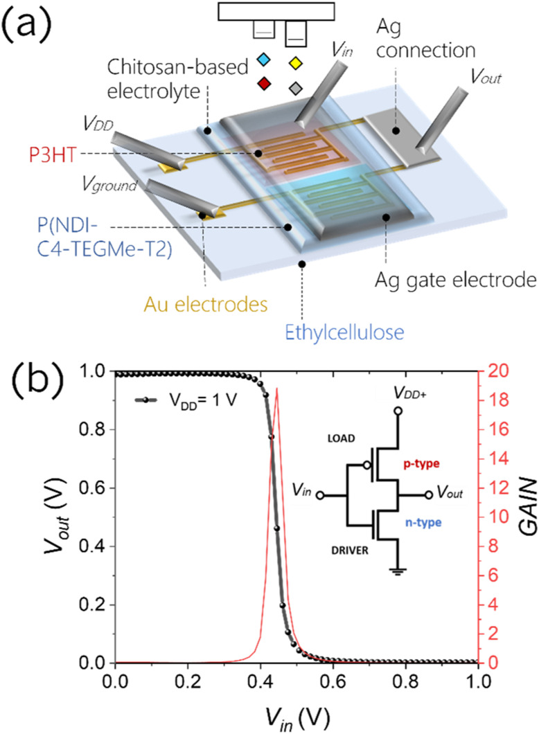
Edible electronics is an emerging research field targeting electronic devices that can be safely ingested and directly digested or metabolized by the human body. As such, it paves the way to a whole new family of applications, ranging from ingestible medical devices and biosensors to smart labelling for food quality monitoring and anti-counterfeiting. Being a newborn research field, many challenges need to be addressed to realize fully edible electronic components. In particular, an extended library of edible electronic materials is required, with suitable electronic properties depending on the target device and compatible with large-area printing processes, to allow scalable and cost-effective manufacturing. In this work, we propose a platform for future low-voltage edible transistors and circuits that comprises an edible chitosan gating medium and inkjet-printed inert gold electrodes, compatible with low thermal budget edible substrates, such as ethylcellulose. We report the compatibility of the platform, characterized by critical channel features as low as 10 μm, with different inkjet-printed carbon-based semiconductors, including biocompatible polymers present in the picogram range per device. A complementary organic inverter is also demonstrated with the same platform as a proof-of-principle logic gate. The presented results offer a promising approach to future low-voltage edible active circuitry, as well as a testbed for non-toxic printable semiconductors.
可食用电子学是一个新兴的研究领域,针对的是可以安全摄入并被人体直接消化或代谢的电子设备。因此,它为一系列全新的应用铺平了道路,从可食用医疗设备和生物传感器到食品质量监测和防伪的智能标签。作为一个新生的研究领域,要实现完全可食用的电子元件还需要解决许多挑战。特别是需要扩展可食用电子材料的库,这些材料具有适合目标设备的合适电子特性,并与大面积印刷工艺兼容,以实现可扩展和具有成本效益的制造。在这项工作中,我们提出了一个未来低电压可食用晶体管和电路的平台,该平台由可食用壳聚糖门控介质和喷墨打印惰性金电极组成,与低热预算可食用基底(如乙基纤维素)兼容。我们报告了该平台的兼容性,其特征为低至 10μm 的关键通道特性,与不同的喷墨打印碳基半导体兼容,包括每个设备中存在的生物相容性聚合物在皮克级范围内。还使用相同的平台演示了互补有机逆变器,作为原理验证逻辑门。所呈现的结果为未来低电压可食用有源电路提供了有前途的方法,并且为无毒可打印半导体提供了测试平台。