• 文献检索
  • 文档翻译
  • 深度研究
  • 学术资讯
  • Suppr Zotero 插件Zotero 插件
  • 邀请有礼
  • 套餐&价格
  • 历史记录
应用&插件
Suppr Zotero 插件Zotero 插件浏览器插件Mac 客户端Windows 客户端微信小程序
定价
高级版会员购买积分包购买API积分包
服务
文献检索文档翻译深度研究API 文档MCP 服务
关于我们
关于 Suppr公司介绍联系我们用户协议隐私条款
关注我们

Suppr 超能文献

核心技术专利:CN118964589B侵权必究
粤ICP备2023148730 号-1Suppr @ 2026

文献检索

告别复杂PubMed语法,用中文像聊天一样搜索,搜遍4000万医学文献。AI智能推荐,让科研检索更轻松。

立即免费搜索

文件翻译

保留排版,准确专业,支持PDF/Word/PPT等文件格式,支持 12+语言互译。

免费翻译文档

深度研究

AI帮你快速写综述,25分钟生成高质量综述,智能提取关键信息,辅助科研写作。

立即免费体验

碳化硅技术概述:现状、挑战、关键驱动因素及产品路线图。

The Overview of Silicon Carbide Technology: Status, Challenges, Key Drivers, and Product Roadmap.

作者信息

Kamiński Maciej, Król Krystian, Kwietniewski Norbert, Myśliwiec Marcin, Sochacki Mariusz, Stonio Bartłomiej, Kisiel Ryszard, Martychowiec Agnieszka, Racka-Szmidt Katarzyna, Werbowy Aleksander, Żelazko Jarosław, Niedzielski Piotr, Szmidt Jan, Strójwąs Andrzej

机构信息

Institute of Microelectronics and Optoelectronics, Warsaw University of Technology, 75 Koszykowa Str., 00-662 Warsaw, Poland.

Łukasiewicz Research Network-Institute of Microelectronics and Photonics, 32/46 Al. Lotników, 02-668 Warsaw, Poland.

出版信息

Materials (Basel). 2024 Dec 24;18(1):12. doi: 10.3390/ma18010012.

DOI:10.3390/ma18010012
PMID:39795657
原文链接:https://pmc.ncbi.nlm.nih.gov/articles/PMC11721906/
Abstract

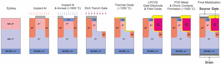
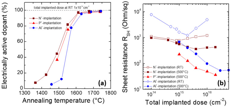
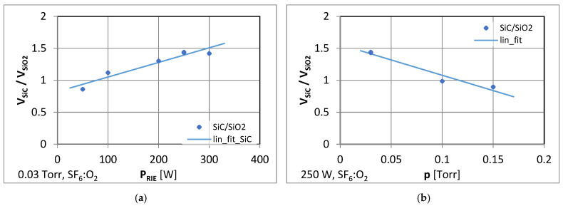
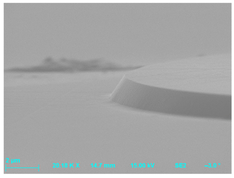
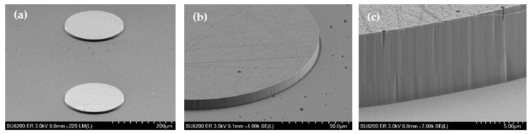
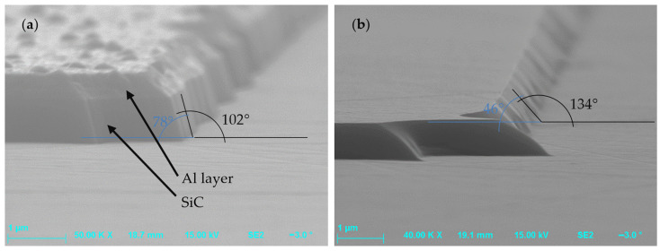
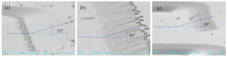
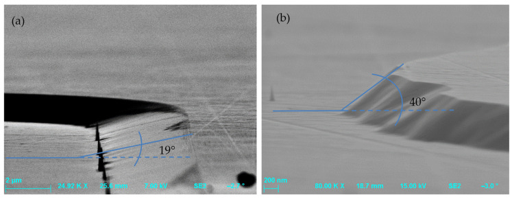
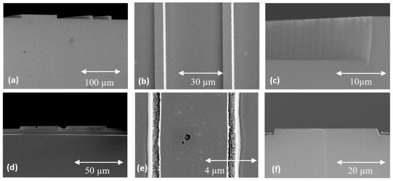
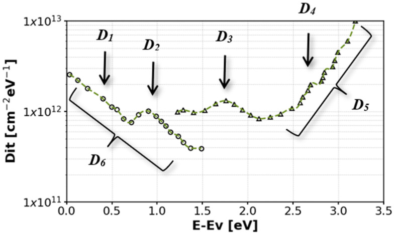
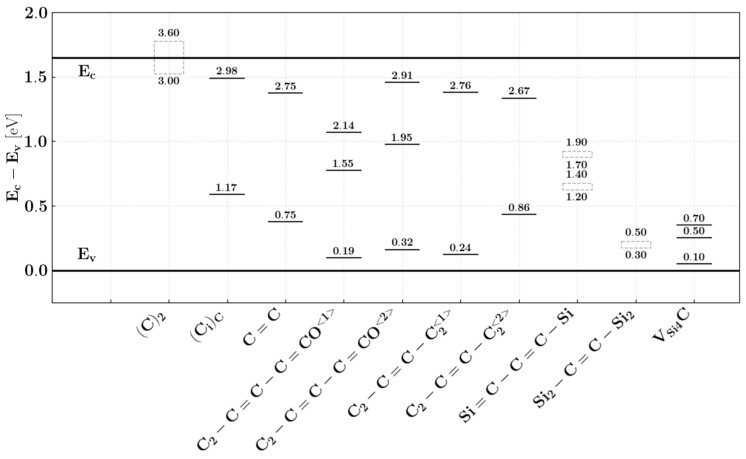
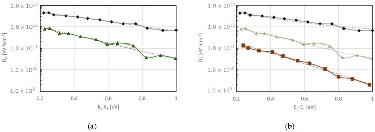
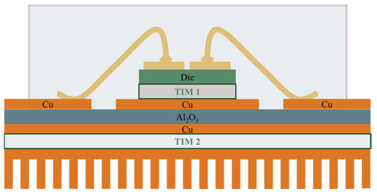
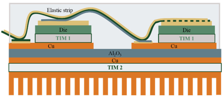
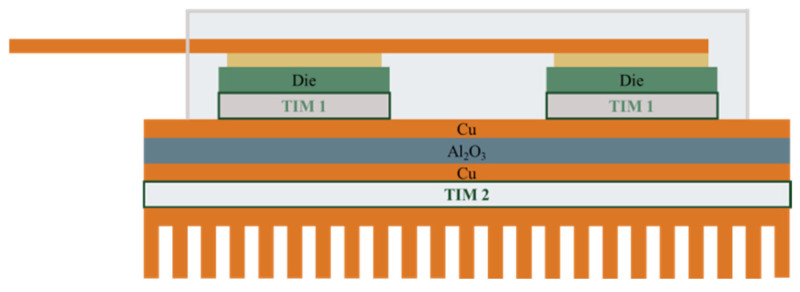
Arguably, SiC technology is the most rapidly expanding IC manufacturing technology driven mostly by the aggressive roadmap for battery electric vehicle penetration and also industrial high-voltage/high-power applications. This paper provides a comprehensive overview of the state of the art of SiC technology focusing on the challenges starting from the difficult and lengthy SiC substrate growth all the way to the complex MOSFET assembly processes. We focus on the differentiation from the established Si manufacturing processes and provide a comprehensive list of references as well as a brief description of our own research into the key manufacturing processes in this technology. We also present a SiC technology and product roadmap.

摘要

可以说,碳化硅(SiC)技术是发展最为迅速的集成电路制造技术,这主要得益于电池电动汽车普及的激进路线图以及工业高压/高功率应用。本文全面概述了SiC技术的现状,重点关注从困难且漫长的SiC衬底生长到复杂的MOSFET组装工艺等一系列挑战。我们着重阐述了与成熟的硅制造工艺的差异,提供了一份全面的参考文献列表,并简要介绍了我们自己对该技术关键制造工艺的研究。我们还展示了一份SiC技术和产品路线图。

https://cdn.ncbi.nlm.nih.gov/pmc/blobs/6455/11721906/8949e1235409/materials-18-00012-g021.jpg
https://cdn.ncbi.nlm.nih.gov/pmc/blobs/6455/11721906/50d572ec86dc/materials-18-00012-g001.jpg
https://cdn.ncbi.nlm.nih.gov/pmc/blobs/6455/11721906/ea57e96bf684/materials-18-00012-g002.jpg
https://cdn.ncbi.nlm.nih.gov/pmc/blobs/6455/11721906/6ba4cc69ef65/materials-18-00012-g003.jpg
https://cdn.ncbi.nlm.nih.gov/pmc/blobs/6455/11721906/9bc7801fe5d9/materials-18-00012-g004.jpg
https://cdn.ncbi.nlm.nih.gov/pmc/blobs/6455/11721906/1fafa247eea4/materials-18-00012-g005.jpg
https://cdn.ncbi.nlm.nih.gov/pmc/blobs/6455/11721906/fc93172c2aff/materials-18-00012-g006.jpg
https://cdn.ncbi.nlm.nih.gov/pmc/blobs/6455/11721906/3e0265ecfeda/materials-18-00012-g007.jpg
https://cdn.ncbi.nlm.nih.gov/pmc/blobs/6455/11721906/cb9d23d4822e/materials-18-00012-g008.jpg
https://cdn.ncbi.nlm.nih.gov/pmc/blobs/6455/11721906/00daedc4d5cc/materials-18-00012-g009.jpg
https://cdn.ncbi.nlm.nih.gov/pmc/blobs/6455/11721906/69376938f5e5/materials-18-00012-g010.jpg
https://cdn.ncbi.nlm.nih.gov/pmc/blobs/6455/11721906/d5cdaae4c7b4/materials-18-00012-g011.jpg
https://cdn.ncbi.nlm.nih.gov/pmc/blobs/6455/11721906/15b8fd2bf384/materials-18-00012-g012.jpg
https://cdn.ncbi.nlm.nih.gov/pmc/blobs/6455/11721906/e1eb85b80b1f/materials-18-00012-g013.jpg
https://cdn.ncbi.nlm.nih.gov/pmc/blobs/6455/11721906/07120c3638fb/materials-18-00012-g014.jpg
https://cdn.ncbi.nlm.nih.gov/pmc/blobs/6455/11721906/bf8f388a979c/materials-18-00012-g015.jpg
https://cdn.ncbi.nlm.nih.gov/pmc/blobs/6455/11721906/a26d147904e1/materials-18-00012-g016.jpg
https://cdn.ncbi.nlm.nih.gov/pmc/blobs/6455/11721906/12afd0528b45/materials-18-00012-g017.jpg
https://cdn.ncbi.nlm.nih.gov/pmc/blobs/6455/11721906/af4f0ff4f999/materials-18-00012-g018.jpg
https://cdn.ncbi.nlm.nih.gov/pmc/blobs/6455/11721906/91f61a2b0412/materials-18-00012-g019.jpg
https://cdn.ncbi.nlm.nih.gov/pmc/blobs/6455/11721906/f1e05eb08775/materials-18-00012-g020.jpg
https://cdn.ncbi.nlm.nih.gov/pmc/blobs/6455/11721906/8949e1235409/materials-18-00012-g021.jpg

相似文献

1
The Overview of Silicon Carbide Technology: Status, Challenges, Key Drivers, and Product Roadmap.碳化硅技术概述:现状、挑战、关键驱动因素及产品路线图。
Materials (Basel). 2024 Dec 24;18(1):12. doi: 10.3390/ma18010012.
2
Status and Prospects of Cubic Silicon Carbide Power Electronics Device Technology.立方碳化硅功率电子器件技术的现状与展望
Materials (Basel). 2021 Oct 5;14(19):5831. doi: 10.3390/ma14195831.
3
Power Electronics Revolutionized: A Comprehensive Analysis of Emerging Wide and Ultrawide Bandgap Devices.电力电子学的变革:对新兴宽禁带和超宽禁带器件的全面分析。
Micromachines (Basel). 2023 Oct 31;14(11):2045. doi: 10.3390/mi14112045.
4
Characteristics of a 1200 V Hybrid Power Switch Comprising a Si IGBT and a SiC MOSFET.一种包含硅绝缘栅双极型晶体管(Si IGBT)和碳化硅金属氧化物半导体场效应晶体管(SiC MOSFET)的1200伏混合功率开关的特性
Micromachines (Basel). 2024 Oct 31;15(11):1337. doi: 10.3390/mi15111337.
5
Selective Doping in Silicon Carbide Power Devices.碳化硅功率器件中的选择性掺杂
Materials (Basel). 2021 Jul 14;14(14):3923. doi: 10.3390/ma14143923.
6
Design of 400 V Miniature DC Solid State Circuit Breaker with SiC MOSFET.采用碳化硅金属氧化物半导体场效应晶体管的400V微型直流固态断路器设计
Micromachines (Basel). 2019 May 10;10(5):314. doi: 10.3390/mi10050314.
7
Novel Photonic Applications of Silicon Carbide.碳化硅的新型光子应用
Materials (Basel). 2023 Jan 22;16(3):1014. doi: 10.3390/ma16031014.
8
Fundamental research on semiconductor SiC and its applications to power electronics.半导体碳化硅的基础研究及其在电力电子学中的应用。
Proc Jpn Acad Ser B Phys Biol Sci. 2020;96(7):235-254. doi: 10.2183/pjab.96.018.
9
A Two-Dimensional Computer-Aided Design Study of Unclamped Inductive Switching in an Improved 4H-SiC VDMOSFET.一种改进型4H-SiC VDMOSFET中无钳位电感开关的二维计算机辅助设计研究
Micromachines (Basel). 2023 Dec 23;15(1):35. doi: 10.3390/mi15010035.
10
Materials and Processes for Schottky Contacts on Silicon Carbide.碳化硅肖特基接触的材料与工艺
Materials (Basel). 2021 Dec 31;15(1):298. doi: 10.3390/ma15010298.

本文引用的文献

1
Carrier Trap Density Reduction at SiO/4H-Silicon Carbide Interface with Annealing Processes in Phosphoryl Chloride and Nitride Oxide Atmospheres.通过在磷酰氯和氮氧化物气氛中进行退火工艺降低SiO/4H-碳化硅界面处的载流子陷阱密度
Materials (Basel). 2023 Jun 14;16(12):4381. doi: 10.3390/ma16124381.
2
A Review: Inductively Coupled Plasma Reactive Ion Etching of Silicon Carbide.综述:碳化硅的电感耦合等离子体反应离子刻蚀
Materials (Basel). 2021 Dec 24;15(1):123. doi: 10.3390/ma15010123.
3
Recent Advances in Reactive Ion Etching and Applications of High-Aspect-Ratio Microfabrication.
反应离子蚀刻的最新进展及高深宽比微纳加工的应用
Micromachines (Basel). 2021 Aug 20;12(8):991. doi: 10.3390/mi12080991.
4
Selective Doping in Silicon Carbide Power Devices.碳化硅功率器件中的选择性掺杂
Materials (Basel). 2021 Jul 14;14(14):3923. doi: 10.3390/ma14143923.
5
The Impact of Process Conditions on Surge Current Capability of 1.2 kV SiC JBS and MPS Diodes.工艺条件对1.2 kV碳化硅结势垒肖特基(JBS)二极管和MPS二极管浪涌电流能力的影响
Materials (Basel). 2021 Jan 31;14(3):663. doi: 10.3390/ma14030663.
6
Characterization and Fabrication of the CFM-JTE for 4H-SiC Power Device with High-Efficiency Protection and Increased JTE Dose Tolerance Window.用于4H-SiC功率器件的具有高效保护和增加JTE剂量耐受窗口的CFM-JTE的特性与制造
Nanoscale Res Lett. 2020 Nov 10;15(1):211. doi: 10.1186/s11671-020-03443-5.
7
4H-SiC surface morphology after Al ion implantation and annealing with C-cap.铝离子注入并采用碳帽退火后的4H-碳化硅表面形貌
J Microsc. 2020 Dec;280(3):229-240. doi: 10.1111/jmi.12933. Epub 2020 Jun 19.
8
Laser Annealing of P and Al Implanted 4H-SiC Epitaxial Layers.磷和铝离子注入的4H-SiC外延层的激光退火
Materials (Basel). 2019 Oct 15;12(20):3362. doi: 10.3390/ma12203362.
9
Vertical and bevel-structured SiC etching techniques incorporating different gas mixture plasmas for various microelectronic applications.采用不同混合气体等离子体的垂直和斜面结构化碳化硅刻蚀技术,适用于各种微电子应用。
Sci Rep. 2017 Jun 20;7(1):3915. doi: 10.1038/s41598-017-04389-y.
10
Surface cleaning and etching of 4H-SiC(0001) using high-density atmospheric pressure hydrogen plasma.使用高密度大气压氢等离子体对4H-SiC(0001)进行表面清洁和蚀刻。
J Nanosci Nanotechnol. 2011 Apr;11(4):2802-8. doi: 10.1166/jnn.2011.3911.