Kumar Prabhukrupa Chinmay, Mohanty Subhashree, Panda Jnanranjan, Das Subhashree, Supriya Swikruti, Alagarasan Devarajan, Naik Ramakanta
Department of Engineering and Materials Physics, Institute of Chemical Technology-Indian Oil Odisha Campus Bhubaneswar 751013 India
Faculty of Science, Sri Sri University Cuttack 754006 India.
RSC Adv. 2025 May 6;15(18):14518-14531. doi: 10.1039/d5ra00917k. eCollection 2025 Apr 28.
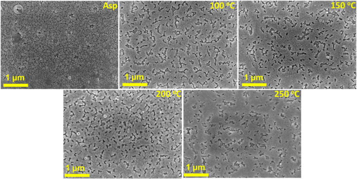
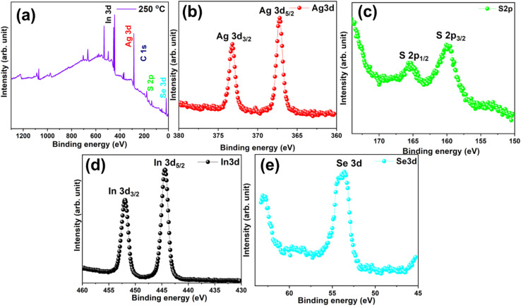
AgS and InSe, two prominent functional materials, have recently gained extensive research attention. AgS shows good chemical stability with excellent photoconducting ability as a direct, narrow band-gap semiconductor. InSe compounds have been widely used in optoelectronics, photodetectors, and gas sensors. In this work, we develop a visible light photodetector by combining these two materials from AgS/InSe heterostructure films at room temperature. The AgS/InSe bilayer films were annealed at different temperatures, and their photodetection parameters were compared to different annealed films. The bilayer structure and the interdiffusion of AgS into the InSe layer were confirmed through a cross-sectional FESEM view. The 250 °C annealed sample shows better photoconductivity with a maximum responsivity of 2.01 × 10 A/W and 7.32 × 10 Jones of detectivity than the other films. The current increase from nA to mA upon annealing significantly increased the photo response of the 250 °C annealed films. The hydrophilic properties improved with annealing, as confirmed by contact angle measurement. It is also further verified by the increased porosity observed from the FESEM images of the surface morphology. The transition from amorphous to polycrystalline was confirmed through XRD. The interdiffusion by annealing resulted in the formation of ternary phases like AgInS and AgInSe as seen from the XRD and HRTEM data. The crystallite size that increased upon annealing reduced the dislocation density from 3.29 × 10 to 2.73 × 10 m. The optical bandgap, density, extinction coefficient, and skin depth showed changes as probed by UV-visible spectroscopy. Upon annealing, the band gap was enhanced by 0.157 eV from its as-prepared state. The observed changes in optical parameters and photoconductivity make the film a suitable candidate for visible light photodetection.
硫化银(AgS)和硒化铟(InSe)这两种重要的功能材料最近受到了广泛的研究关注。硫化银作为一种直接带隙窄的半导体,具有良好的化学稳定性和优异的光电导能力。硒化铟化合物已广泛应用于光电子学、光电探测器和气体传感器领域。在本工作中,我们在室温下通过将这两种材料组合成硫化银/硒化铟异质结构薄膜来制备一种可见光光电探测器。对硫化银/硒化铟双层薄膜在不同温度下进行退火处理,并将其光电探测参数与不同退火温度的薄膜进行比较。通过横截面场发射扫描电子显微镜(FESEM)观察确认了双层结构以及硫化银向硒化铟层的相互扩散。与其他薄膜相比,250℃退火的样品表现出更好的光电导性,最大响应率为2.01×10 A/W,探测率为7.32×10琼斯。退火后电流从纳安增加到毫安,显著提高了250℃退火薄膜的光响应。通过接触角测量证实,退火后亲水性得到改善。表面形貌的FESEM图像显示孔隙率增加,这也进一步证实了这一点。通过X射线衍射(XRD)确认了从非晶到多晶的转变。从XRD和高分辨率透射电子显微镜(HRTEM)数据可以看出,退火导致的相互扩散形成了三元相,如AgInS和AgInSe。退火后增加的微晶尺寸使位错密度从3.29×10降至2.73×10 m。通过紫外-可见光谱探测发现,光学带隙、密度、消光系数和趋肤深度都发生了变化。退火后,带隙比制备态提高了0.157 eV。观察到的光学参数和光电导性的变化使该薄膜成为可见光光电探测的合适候选材料。