• 文献检索
  • 文档翻译
  • 深度研究
  • 学术资讯
  • Suppr Zotero 插件Zotero 插件
  • 邀请有礼
  • 套餐&价格
  • 历史记录
应用&插件
Suppr Zotero 插件Zotero 插件浏览器插件Mac 客户端Windows 客户端微信小程序
定价
高级版会员购买积分包购买API积分包
服务
文献检索文档翻译深度研究API 文档MCP 服务
关于我们
关于 Suppr公司介绍联系我们用户协议隐私条款
关注我们

Suppr 超能文献

核心技术专利:CN118964589B侵权必究
粤ICP备2023148730 号-1Suppr @ 2026

文献检索

告别复杂PubMed语法,用中文像聊天一样搜索,搜遍4000万医学文献。AI智能推荐,让科研检索更轻松。

立即免费搜索

文件翻译

保留排版,准确专业,支持PDF/Word/PPT等文件格式,支持 12+语言互译。

免费翻译文档

深度研究

AI帮你快速写综述,25分钟生成高质量综述,智能提取关键信息,辅助科研写作。

立即免费体验

具有超低暗电流和高响应度的外延石墨烯/n型硅光电二极管

Epitaxial Graphene/n-Si Photodiode with Ultralow Dark Current and High Responsivity.

作者信息

Yin Lanxin, Wang Xiaoyue, Feng Shun

机构信息

College of Information Science and Engineering, Northeastern University, Shenyang 110819, China.

Shenyang National Laboratory for Materials Science, Institute of Metal Research, Chinese Academy of Sciences, 72 Wenhua Road, Shenyang 110016, China.

出版信息

Nanomaterials (Basel). 2025 Aug 3;15(15):1190. doi: 10.3390/nano15151190.

DOI:10.3390/nano15151190
PMID:40801728
原文链接:https://pmc.ncbi.nlm.nih.gov/articles/PMC12348325/
Abstract

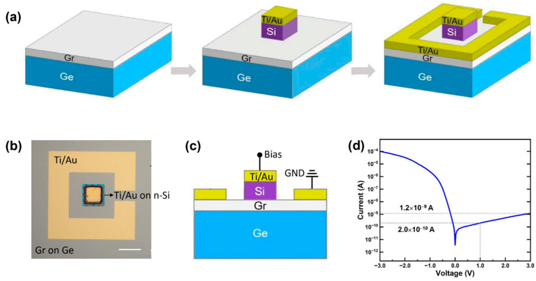
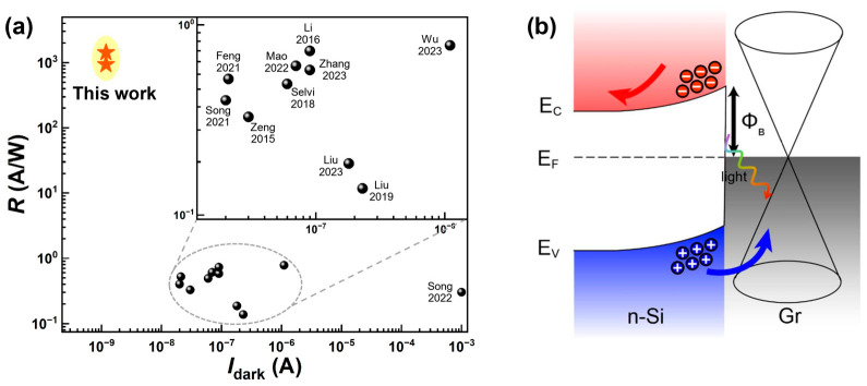
Graphene's exceptional carrier mobility and broadband absorption make it promising for ultrafast photodetection. However, its low optical absorption limits responsivity, while the absence of a bandgap results in high dark current, constraining the signal-to-noise ratio and efficiency. Although silicon (Si) photodetectors normally offer fabrication compatibility, their performance is severely hindered by interface trap states and optical shading. To overcome these limitations, we demonstrate an epitaxial graphene/n-Si heterojunction photodiode. This device utilizes graphene epitaxially grown on germanium integrated with a transferred Si thin film, eliminating polymer residues and interface defects common in transferred graphene. As a result, the fabricated photodetector achieves an ultralow dark current of 1.2 × 10 A, a high responsivity of 1430 A/W, and self-powered operation at room temperature. This work provides a strategy for high-sensitivity and low-power photodetection and demonstrates the practical integration potential of graphene/Si heterostructures for advanced optoelectronics.

摘要

石墨烯卓越的载流子迁移率和宽带吸收特性使其在超快光电探测方面颇具潜力。然而,其低光吸收率限制了响应度,而缺乏带隙则导致暗电流较高,从而限制了信噪比和效率。尽管硅(Si)光电探测器通常具有制造兼容性,但其性能受到界面陷阱态和光学遮蔽的严重阻碍。为克服这些限制,我们展示了一种外延石墨烯/n-Si异质结光电二极管。该器件利用外延生长在锗上的石墨烯与转移的Si薄膜集成,消除了转移石墨烯中常见的聚合物残留和界面缺陷。结果,所制备的光电探测器实现了1.2×10 A的超低暗电流、1430 A/W的高响应度以及室温下的自供电运行。这项工作为高灵敏度和低功耗光电探测提供了一种策略,并展示了石墨烯/Si异质结构在先进光电子学中的实际集成潜力。

https://cdn.ncbi.nlm.nih.gov/pmc/blobs/ab41/12348325/6517c2e2b0ba/nanomaterials-15-01190-g004.jpg
https://cdn.ncbi.nlm.nih.gov/pmc/blobs/ab41/12348325/0d89770a19a3/nanomaterials-15-01190-g001.jpg
https://cdn.ncbi.nlm.nih.gov/pmc/blobs/ab41/12348325/c83c35ffff72/nanomaterials-15-01190-g002.jpg
https://cdn.ncbi.nlm.nih.gov/pmc/blobs/ab41/12348325/966589243255/nanomaterials-15-01190-g003.jpg
https://cdn.ncbi.nlm.nih.gov/pmc/blobs/ab41/12348325/6517c2e2b0ba/nanomaterials-15-01190-g004.jpg

相似文献

1
Epitaxial Graphene/n-Si Photodiode with Ultralow Dark Current and High Responsivity.具有超低暗电流和高响应度的外延石墨烯/n型硅光电二极管
Nanomaterials (Basel). 2025 Aug 3;15(15):1190. doi: 10.3390/nano15151190.
2
On-chip graphene photodetectors with a nonvolatile p-i-n homojunction.具有非易失性p-i-n同质结的片上石墨烯光电探测器。
Light Sci Appl. 2025 Jul 7;14(1):238. doi: 10.1038/s41377-025-01832-y.
3
Enhancing the photoresponse performance of graphene on silicon-based heterojunction as a broadband photodetector.增强石墨烯在硅基异质结上作为宽带光电探测器的光响应性能。
Sci Rep. 2025 Jul 25;15(1):27139. doi: 10.1038/s41598-025-13266-y.
4
Waveguide-integrated PdSe/MoS van der Waals heterojunction photodetector on a thin-film lithium niobate platform.基于薄膜铌酸锂平台的波导集成PdSe/MoS范德华异质结光电探测器。
Appl Opt. 2025 Jun 20;64(18):5115-5120. doi: 10.1364/AO.564072.
5
Prescription of Controlled Substances: Benefits and Risks管制药品的处方:益处与风险
6
Solution-Processable Van Der Waals Heterojunctions on Silicon for Self-Powered Photodetectors with High Responsivity and Detectivity.用于具有高响应度和探测率的自供电光电探测器的硅基溶液可加工范德华异质结
Adv Sci (Weinh). 2025 Jun;12(23):e2500027. doi: 10.1002/advs.202500027. Epub 2025 Mar 28.
7
Voltage-tunable side-illuminated graphene-InP Schottky photodetector with enhanced responsivity through multi-layer graphene integration.通过多层石墨烯集成实现具有增强响应度的电压可调侧面照明石墨烯-磷化铟肖特基光电探测器。
Appl Opt. 2025 Jun 1;64(16):4464-4473. doi: 10.1364/AO.563781.
8
High-Performance UV-Visible Dual-Band Self-Powered Photodetector Based on ZnO/BFZO/P3HT Heterojunction for Logic Gates and Encrypted Communication.基于ZnO/BFZO/P3HT异质结的高性能紫外-可见双波段自供电光电探测器用于逻辑门和加密通信
ACS Appl Mater Interfaces. 2025 Jul 30;17(30):43235-43244. doi: 10.1021/acsami.5c09158. Epub 2025 Jul 18.
9
High-Performance Broadband Integrated Detection System for Multifunctional Applications.用于多功能应用的高性能宽带集成检测系统
ACS Nano. 2025 Jun 24;19(24):22414-22423. doi: 10.1021/acsnano.5c06392. Epub 2025 Jun 12.
10
Interface Engineering of π-Conjugated Conducting Metal-Organic Frameworks for Multiband Self-Powered Photodetector.用于多波段自供电光电探测器的π共轭导电金属有机框架的界面工程
ACS Appl Mater Interfaces. 2025 Jun 25;17(25):36934-36942. doi: 10.1021/acsami.5c06272. Epub 2025 Jun 11.

本文引用的文献

1
Recent Developments of Advanced Broadband Photodetectors Based on 2D Materials.基于二维材料的先进宽带光电探测器的最新进展
Nanomaterials (Basel). 2025 Mar 11;15(6):431. doi: 10.3390/nano15060431.
2
High-sensitivity, high-speed, broadband mid-infrared photodetector enabled by a van der Waals heterostructure with a vertical transport channel.由具有垂直传输通道的范德华异质结构实现的高灵敏度、高速、宽带中红外光电探测器。
Nat Commun. 2025 Jan 10;16(1):564. doi: 10.1038/s41467-025-55887-x.
3
Advances in the Field of Two-Dimensional Crystal-Based Photodetectors.
基于二维晶体的光电探测器领域的进展
Nanomaterials (Basel). 2023 Apr 15;13(8):1379. doi: 10.3390/nano13081379.
4
High-performance gold/graphene/germanium photodetector based on a graphene-on-germanium wafer.基于锗基石墨烯晶圆的高性能金/石墨烯/锗光电探测器。
Nanotechnology. 2022 Jun 7;33(34). doi: 10.1088/1361-6528/ac6ff0.
5
A Broadband Photoelectronic Detector in a Silicon Nanopillar Array with High Detectivity Enhanced by a Monolayer Graphene.一种具有单层石墨烯增强高探测率的硅纳米柱阵列宽带光电子探测器。
Nano Lett. 2021 Jul 14;21(13):5655-5662. doi: 10.1021/acs.nanolett.1c01244. Epub 2021 Jun 28.
6
Interface Engineering Ti C MXene/Silicon Self-Powered Photodetectors with High Responsivity and Detectivity for Weak Light Applications.用于弱光应用的具有高响应度和探测率的界面工程化Ti C MXene/硅自供电光电探测器
Small. 2021 Jun;17(23):e2100439. doi: 10.1002/smll.202100439. Epub 2021 Apr 23.
7
Interface Engineering-Assisted 3D-Graphene/Germanium Heterojunction for High-Performance Photodetectors.界面工程辅助的用于高性能光电探测器的3D石墨烯/锗异质结
ACS Appl Mater Interfaces. 2020 Apr 1;12(13):15606-15614. doi: 10.1021/acsami.0c02485. Epub 2020 Mar 19.
8
Infrared Photodetector Based on the Photothermionic Effect of Graphene-Nanowall/Silicon Heterojunction.基于石墨烯-纳米壁/硅异质结光热电子效应的红外光电探测器
ACS Appl Mater Interfaces. 2019 May 15;11(19):17663-17669. doi: 10.1021/acsami.9b03329. Epub 2019 Apr 30.
9
Seamless lateral graphene p-n junctions formed by selective in situ doping for high-performance photodetectors.通过选择性原位掺杂形成的用于高性能光电探测器的无缝横向石墨烯 p-n 结。
Nat Commun. 2018 Dec 5;9(1):5168. doi: 10.1038/s41467-018-07555-6.
10
Recent Progress and Future Prospects of 2D-Based Photodetectors.二维基光电探测器的最新进展和未来展望。
Adv Mater. 2018 Dec;30(51):e1801164. doi: 10.1002/adma.201801164. Epub 2018 Jul 31.