• 文献检索
  • 文档翻译
  • 深度研究
  • 学术资讯
  • Suppr Zotero 插件Zotero 插件
  • 邀请有礼
  • 套餐&价格
  • 历史记录
应用&插件
Suppr Zotero 插件Zotero 插件浏览器插件Mac 客户端Windows 客户端微信小程序
定价
高级版会员购买积分包购买API积分包
服务
文献检索文档翻译深度研究API 文档MCP 服务
关于我们
关于 Suppr公司介绍联系我们用户协议隐私条款
关注我们

Suppr 超能文献

核心技术专利:CN118964589B侵权必究
粤ICP备2023148730 号-1Suppr @ 2026

文献检索

告别复杂PubMed语法,用中文像聊天一样搜索,搜遍4000万医学文献。AI智能推荐,让科研检索更轻松。

立即免费搜索

文件翻译

保留排版,准确专业,支持PDF/Word/PPT等文件格式,支持 12+语言互译。

免费翻译文档

深度研究

AI帮你快速写综述,25分钟生成高质量综述,智能提取关键信息,辅助科研写作。

立即免费体验

在塑料衬底上实现灵活可调谐的硅光子电路。

Flexible and tunable silicon photonic circuits on plastic substrates.

机构信息

Department of Electrical and Computer Engineering, University of Minnesota, Minneapolis, MN 55455, USA.

出版信息

Sci Rep. 2012;2:622. doi: 10.1038/srep00622. Epub 2012 Sep 3.

DOI:10.1038/srep00622
PMID:22953043
原文链接:https://pmc.ncbi.nlm.nih.gov/articles/PMC3432454/
Abstract

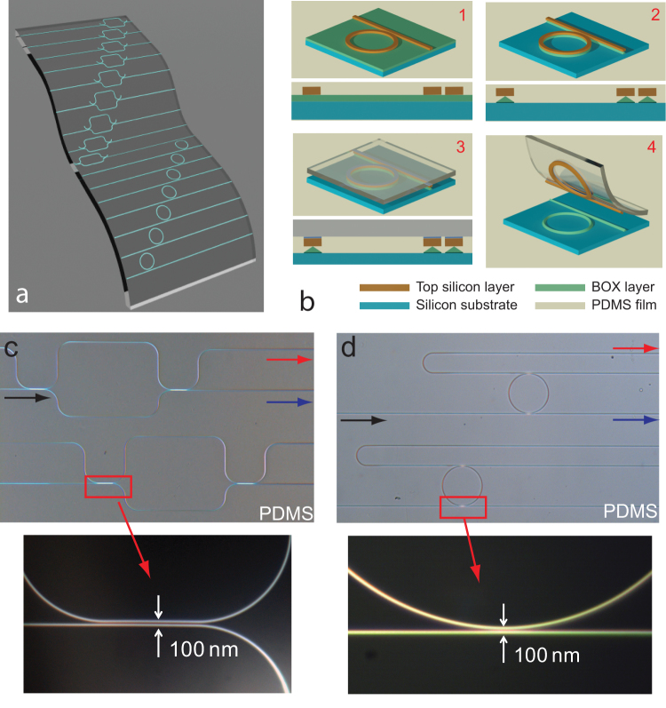
Flexible microelectronics has shown tremendous promise in a broad spectrum of applications, especially those that cannot be addressed by conventional microelectronics in rigid materials and constructions. These unconventional yet important applications range from flexible consumer electronics to conformal sensor arrays and biomedical devices. A recent paradigm shift in implementing flexible electronics is to physically transfer highly integrated devices made in high-quality, crystalline semiconductors on to plastic substrates. Here we demonstrate a flexible form of silicon photonics using the transfer-and-bond fabrication method. Photonic circuits including interferometers and resonators have been transferred onto flexible plastic substrates with preserved functionalities and performance. By mechanically deforming, the optical characteristics of the devices can be tuned reversibly over a remarkably large range. The demonstration of the new flexible photonic systems based on the silicon-on-plastic (SOP) platform could open the door to many future applications, including tunable photonics, optomechanical sensors and biomechanical and bio-photonic probes.

摘要

柔性微电子在广泛的应用中展现出了巨大的潜力,尤其是在传统微电子学无法应用于刚性材料和结构的领域。这些非传统但重要的应用包括从柔性消费电子产品到共形传感器阵列和生物医学设备。最近,在实现柔性电子产品方面出现了一种新的范例转变,即将高质量、结晶半导体制成的高度集成器件物理转移到塑料衬底上。在这里,我们使用转移和键合制造方法展示了一种柔性形式的硅光子学。包括干涉仪和谐振器在内的光子电路已被转移到具有保留功能和性能的柔性塑料衬底上。通过机械变形,可以在非常大的范围内可逆地调整器件的光学特性。基于硅上塑料(SOP)平台的新型柔性光子系统的演示为许多未来的应用打开了大门,包括可调谐光子学、光机械传感器以及生物力学和生物光子学探头。

https://cdn.ncbi.nlm.nih.gov/pmc/blobs/2f4e/3432454/a6a87c843c60/srep00622-f4.jpg
https://cdn.ncbi.nlm.nih.gov/pmc/blobs/2f4e/3432454/1c2e293cfa8e/srep00622-f1.jpg
https://cdn.ncbi.nlm.nih.gov/pmc/blobs/2f4e/3432454/5d9d4c7514bf/srep00622-f2.jpg
https://cdn.ncbi.nlm.nih.gov/pmc/blobs/2f4e/3432454/2c5e099d1e7a/srep00622-f3.jpg
https://cdn.ncbi.nlm.nih.gov/pmc/blobs/2f4e/3432454/a6a87c843c60/srep00622-f4.jpg

相似文献

1
Flexible and tunable silicon photonic circuits on plastic substrates.在塑料衬底上实现灵活可调谐的硅光子电路。
Sci Rep. 2012;2:622. doi: 10.1038/srep00622. Epub 2012 Sep 3.
2
Integrated silicon and silicon nitride photonic circuits on flexible substrates.柔性衬底上的集成硅和氮化硅光子电路。
Opt Lett. 2014 Jun 15;39(12):3449-52. doi: 10.1364/OL.39.003449.
3
Organic printed photonics: From microring lasers to integrated circuits.有机印刷光子学:从微环激光器到集成电路。
Sci Adv. 2015 Sep 18;1(8):e1500257. doi: 10.1126/sciadv.1500257. eCollection 2015 Sep.
4
Mechanically-flexible wafer-scale integrated-photonics fabrication platform.机械柔性晶圆级集成光子学制造平台。
Sci Rep. 2024 May 9;14(1):10623. doi: 10.1038/s41598-024-61055-w.
5
Ge Ion Implanted Photonic Devices and Annealing for Emerging Applications.用于新兴应用的锗离子注入光子器件及退火处理
Micromachines (Basel). 2022 Feb 12;13(2):291. doi: 10.3390/mi13020291.
6
Passive Photonic Integrated Circuits Elements Fabricated on a Silicon Nitride Platform.基于氮化硅平台制造的无源光子集成电路元件
Materials (Basel). 2022 Feb 14;15(4):1398. doi: 10.3390/ma15041398.
7
Heterogeneously integrated silicon photonics for the mid-infrared and spectroscopic sensing.用于中红外和光谱传感的异质集成硅光子学。
ACS Nano. 2014 Jul 22;8(7):6955-61. doi: 10.1021/nn501765k.
8
Thermal tunable silicon valley photonic crystal ring resonators at the telecommunication wavelength.在电信波长下具有热可调硅谷光子晶体环形谐振器。
Opt Express. 2023 Jan 16;31(2):2807-2815. doi: 10.1364/OE.475559.
9
High Performance MgO-barrier Magnetic Tunnel Junctions for Flexible and Wearable Spintronic Applications.高性能 MgO 势垒磁性隧道结,用于柔性可穿戴自旋电子应用。
Sci Rep. 2017 Feb 2;7:42001. doi: 10.1038/srep42001.
10
High-quality Si3N4 circuits as a platform for graphene-based nanophotonic devices.高质量的氮化硅电路作为基于石墨烯的纳米光子器件的平台。
Opt Express. 2013 Dec 16;21(25):31678-89. doi: 10.1364/OE.21.031678.

引用本文的文献

1
High Q-factor Polymer Microring Resonators Realized by Versatile Damascene Soft Nanoimprinting Lithography.通过通用大马士革软纳米压印光刻技术实现的高Q因子聚合物微环谐振器
Adv Funct Mater. 2024 May 10;34(19). doi: 10.1002/adfm.202312229. Epub 2024 Jan 17.
2
Omnidirectional color wavelength tuning of stretchable chiral liquid crystal elastomers.可拉伸手性液晶弹性体的全向颜色波长调谐
Light Sci Appl. 2024 May 22;13(1):114. doi: 10.1038/s41377-024-01470-w.
3
The Combined Spectral Response of a MEMS Metamaterial Absorber for the Mid-IR and Its Sub-Wavelength Fabrication Residual Array of Holes.

本文引用的文献

1
Flexible plasmonics on unconventional and nonplanar substrates.非传统和非平面衬底上的柔性等离子体学。
Adv Mater. 2011 Oct 11;23(38):4422-30. doi: 10.1002/adma.201102430. Epub 2011 Aug 24.
2
Flexible concentrator photovoltaics based on microscale silicon solar cells embedded in luminescent waveguides.基于嵌入在波导中的微尺度硅太阳能电池的柔性聚光光伏。
Nat Commun. 2011 Jun 14;2:343. doi: 10.1038/ncomms1318.
3
Large-area flexible 3D optical negative index metamaterial formed by nanotransfer printing.大面积柔性 3D 光学负折射率超材料通过纳米压印转移技术形成。
一种用于中红外的MEMS超材料吸收器的组合光谱响应及其亚波长制造剩余孔阵列
Materials (Basel). 2023 Jun 9;16(12):4278. doi: 10.3390/ma16124278.
4
Pressure Sensitive Adhesive Tape: A Versatile Material Platform for Optical Sensors.压敏胶带:用于光学传感器的多功能材料平台。
Sensors (Basel). 2020 Sep 16;20(18):5303. doi: 10.3390/s20185303.
5
Wearable Triboelectric/Aluminum Nitride Nano-Energy-Nano-System with Self-Sustainable Photonic Modulation and Continuous Force Sensing.具有自持续光子调制和连续力传感功能的可穿戴摩擦电/氮化铝纳米能源纳米系统
Adv Sci (Weinh). 2020 Jun 19;7(15):1903636. doi: 10.1002/advs.201903636. eCollection 2020 Aug.
6
FDTD Simulation: Simultaneous Measurement of the Refractive Index and the Pressure Using Microdisk Resonator with Two Whispering-Gallery Modes.时域有限差分法模拟:利用具有两种回音壁模式的微盘谐振器同时测量折射率和压力
Sensors (Basel). 2020 Jul 16;20(14):3955. doi: 10.3390/s20143955.
7
Direct Growth of Light-Emitting III-V Nanowires on Flexible Plastic Substrates.发光III-V族纳米线在柔性塑料基板上的直接生长。
ACS Nano. 2020 Jun 23;14(6):7484-7491. doi: 10.1021/acsnano.0c03184. Epub 2020 May 27.
8
Nanowire Ring Embedded in a Flexible Substrate for Local Strain Detection.嵌入柔性基板用于局部应变检测的纳米线环
Materials (Basel). 2020 Jan 12;13(2):347. doi: 10.3390/ma13020347.
9
Tape nanolithography: a rapid and simple method for fabricating flexible, wearable nanophotonic devices.胶带纳米光刻:一种用于制造柔性、可穿戴纳米光子器件的快速简便方法。
Microsyst Nanoeng. 2018 Oct 8;4:31. doi: 10.1038/s41378-018-0031-4. eCollection 2018.
10
Flexible Mid-infrared Photonic Circuits for Real-time and Label-Free Hydroxyl Compound Detection.用于实时无标记羟基化合物检测的灵活中红外光子电路。
Sci Rep. 2019 Mar 11;9(1):4153. doi: 10.1038/s41598-019-39062-z.
Nat Nanotechnol. 2011 Jun 5;6(7):402-7. doi: 10.1038/nnano.2011.82.
4
Flexible high-performance carbon nanotube integrated circuits.柔性高性能碳纳米管集成电路。
Nat Nanotechnol. 2011 Mar;6(3):156-61. doi: 10.1038/nnano.2011.1. Epub 2011 Feb 6.
5
Ultrathin compound semiconductor on insulator layers for high-performance nanoscale transistors.用于高性能纳米尺度晶体管的超薄复合半导体绝缘体层。
Nature. 2010 Nov 11;468(7321):286-9. doi: 10.1038/nature09541.
6
Highly strained compliant optical metamaterials with large frequency tunability.具有大频率调谐能力的高应变-compliant 光学超材料。
Nano Lett. 2010 Oct 13;10(10):4222-7. doi: 10.1021/nl102684x.
7
Materials and mechanics for stretchable electronics.可拉伸电子产品的材料与力学
Science. 2010 Mar 26;327(5973):1603-7. doi: 10.1126/science.1182383.
8
Losses in single-mode silicon-on-insulator strip waveguides and bends.绝缘体上硅单模条形波导及弯曲处的损耗
Opt Express. 2004 Apr 19;12(8):1622-31. doi: 10.1364/opex.12.001622.
9
Large-scale pattern growth of graphene films for stretchable transparent electrodes.用于可拉伸透明电极的石墨烯薄膜的大规模图案生长。
Nature. 2009 Feb 5;457(7230):706-10. doi: 10.1038/nature07719. Epub 2009 Jan 14.
10
Ultrathin silicon solar microcells for semitransparent, mechanically flexible and microconcentrator module designs.用于半透明、机械柔性和微聚光器模块设计的超薄硅太阳能微电池。
Nat Mater. 2008 Nov;7(11):907-15. doi: 10.1038/nmat2287. Epub 2008 Oct 5.