• 文献检索
  • 文档翻译
  • 深度研究
  • 学术资讯
  • Suppr Zotero 插件Zotero 插件
  • 邀请有礼
  • 套餐&价格
  • 历史记录
应用&插件
Suppr Zotero 插件Zotero 插件浏览器插件Mac 客户端Windows 客户端微信小程序
定价
高级版会员购买积分包购买API积分包
服务
文献检索文档翻译深度研究API 文档MCP 服务
关于我们
关于 Suppr公司介绍联系我们用户协议隐私条款
关注我们

Suppr 超能文献

核心技术专利:CN118964589B侵权必究
粤ICP备2023148730 号-1Suppr @ 2026

文献检索

告别复杂PubMed语法,用中文像聊天一样搜索,搜遍4000万医学文献。AI智能推荐,让科研检索更轻松。

立即免费搜索

文件翻译

保留排版,准确专业,支持PDF/Word/PPT等文件格式,支持 12+语言互译。

免费翻译文档

深度研究

AI帮你快速写综述,25分钟生成高质量综述,智能提取关键信息,辅助科研写作。

立即免费体验

仅通过剥离工艺实现亚 15nm 单晶体管的高密度十字交叉阵列。

High Density Crossbar Arrays with Sub- 15 nm Single Cells via Liftoff Process Only.

机构信息

Nanoelectronics and Nanotechnology Research Group, Department of Electronics and Computer Science, Faculty of Physical Science and Engineering, University of Southampton, University Road, SO17 1BJ, Southampton, United Kingdom.

Southampton Nanofabrication Centre, University of Southampton, Highfield Campus, Southampton SO17 1BJ, UK.

出版信息

Sci Rep. 2016 Sep 2;6:32614. doi: 10.1038/srep32614.

DOI:10.1038/srep32614
PMID:27585643
原文链接:https://pmc.ncbi.nlm.nih.gov/articles/PMC5009344/
Abstract

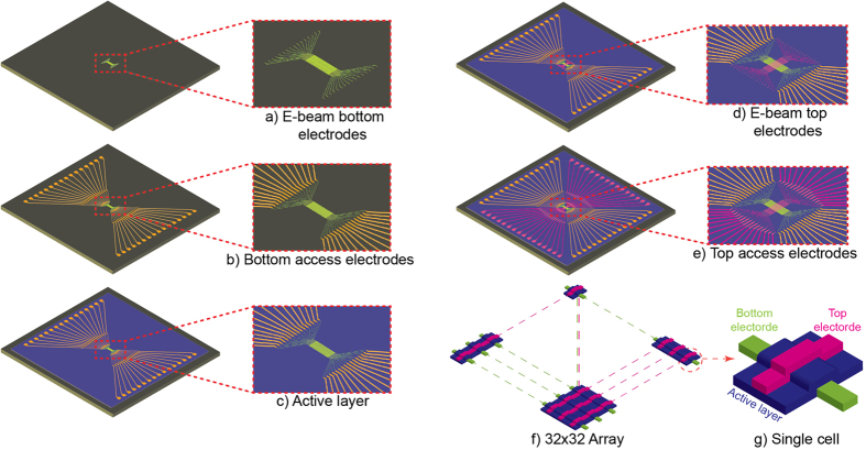
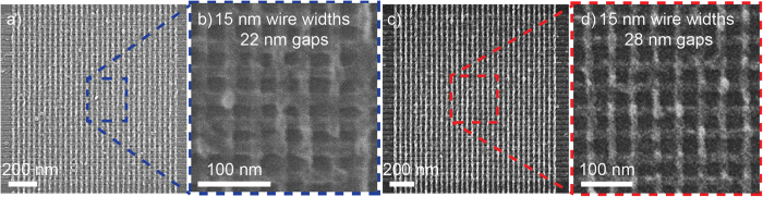
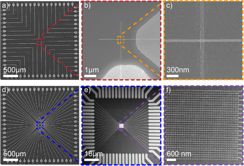
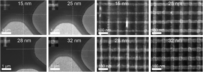
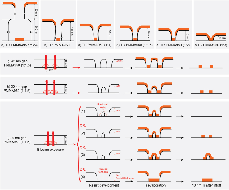
Emerging nano-scale technologies are pushing the fabrication boundaries at their limits, for leveraging an even higher density of nano-devices towards reaching 4F(2)/cell footprint in 3D arrays. Here, we study the liftoff process limits to achieve extreme dense nanowires while ensuring preservation of thin film quality. The proposed method is optimized for attaining a multiple layer fabrication to reliably achieve 3D nano-device stacks of 32 × 32 nanowire arrays across 6-inch wafer, using electron beam lithography at 100 kV and polymethyl methacrylate (PMMA) resist at different thicknesses. The resist thickness and its geometric profile after development were identified to be the major limiting factors, and suggestions for addressing these issues are provided. Multiple layers were successfully achieved to fabricate arrays of 1 Ki cells that have sub- 15 nm nanowires distant by 28 nm across 6-inch wafer.

摘要

新兴的纳米技术正在将制造极限推向极致,以利用更高密度的纳米器件实现 3D 阵列中每单元 4F(2)的面积密度。在这里,我们研究了实现极限提拉工艺的限制,以在确保薄膜质量的同时实现极密集的纳米线。所提出的方法经过优化,可实现多层制造,从而使用 100kV 的电子束光刻和不同厚度的聚甲基丙烯酸甲酯(PMMA)抗蚀剂可靠地实现 32×32 纳米线阵列的 3D 纳米器件堆叠,该方法可在 6 英寸晶圆上实现 32×32 纳米线阵列。抗蚀剂厚度及其在显影后的几何形状被确定为主要的限制因素,并提供了解决这些问题的建议。成功地实现了多层制造,以在 6 英寸晶圆上制造间距为 28nm、线距小于 15nm 的 1Ki 单元的纳米线阵列。

https://cdn.ncbi.nlm.nih.gov/pmc/blobs/c3b0/5009344/4a5f0999cd52/srep32614-f5.jpg
https://cdn.ncbi.nlm.nih.gov/pmc/blobs/c3b0/5009344/5e0140d84382/srep32614-f1.jpg
https://cdn.ncbi.nlm.nih.gov/pmc/blobs/c3b0/5009344/3c9d688ab40a/srep32614-f2.jpg
https://cdn.ncbi.nlm.nih.gov/pmc/blobs/c3b0/5009344/c891ee0aa32b/srep32614-f3.jpg
https://cdn.ncbi.nlm.nih.gov/pmc/blobs/c3b0/5009344/66bfeaf77237/srep32614-f4.jpg
https://cdn.ncbi.nlm.nih.gov/pmc/blobs/c3b0/5009344/4a5f0999cd52/srep32614-f5.jpg

相似文献

1
High Density Crossbar Arrays with Sub- 15 nm Single Cells via Liftoff Process Only.仅通过剥离工艺实现亚 15nm 单晶体管的高密度十字交叉阵列。
Sci Rep. 2016 Sep 2;6:32614. doi: 10.1038/srep32614.
2
Fabrication of sub-10 nm metal nanowire arrays with sub-1 nm critical dimension control.制备具有亚 1nm 临界尺寸控制的亚 10nm 金属纳米线阵列。
Nanotechnology. 2016 Nov 18;27(46):464004. doi: 10.1088/0957-4484/27/46/464004. Epub 2016 Oct 17.
3
Large-scale parallel arrays of silicon nanowires via block copolymer directed self-assembly.通过嵌段共聚物导向自组装制备大规模平行硅纳米线阵列。
Nanoscale. 2012 May 21;4(10):3228-36. doi: 10.1039/c2nr00018k. Epub 2012 Apr 5.
4
Direct e-beam writing of dense and high aspect ratio nanostructures in thick layers of PMMA for electroplating.直接电子束写入 PMMA 厚层中的密集和高纵横比纳米结构,用于电镀。
Nanotechnology. 2010 Jul 23;21(29):295303. doi: 10.1088/0957-4484/21/29/295303. Epub 2010 Jul 5.
5
Batch fabrication of gold-gold nanogaps by E-beam lithography and electrochemical deposition.采用电子束光刻和电化学沉积技术批量制备金-金纳米间隙。
Nanotechnology. 2013 Jun 14;24(23):235302. doi: 10.1088/0957-4484/24/23/235302. Epub 2013 May 15.
6
Fabrication of TiO2 memristive arrays by step and flash imprint lithography.通过步进闪光压印光刻法制备二氧化钛忆阻阵列。
J Nanosci Nanotechnol. 2011 Jan;11(1):696-700. doi: 10.1166/jnn.2011.3282.
7
Mass fabrication of resistive random access crossbar arrays by step and flash imprint lithography.采用步进式和闪光压印光刻技术进行电阻式随机存取交叉点阵列的大规模制造。
Nanotechnology. 2009 Nov 4;20(44):445305. doi: 10.1088/0957-4484/20/44/445305. Epub 2009 Oct 7.
8
Electron beam lithography-assisted fabrication of Au nano-dot array as a substrate of a correlated AFM and confocal Raman spectroscopy.电子束光刻辅助制备金纳米点阵列作为关联原子力显微镜和共焦拉曼光谱的基底。
Ultramicroscopy. 2008 Sep;108(10):1302-6. doi: 10.1016/j.ultramic.2008.04.056. Epub 2008 May 14.
9
Wafer-scale high-throughput ordered arrays of Si and coaxial Si/Si(1-x)Ge(x) wires: fabrication, characterization, and photovoltaic application.晶圆级硅和同轴硅/硅(1-x)锗(x)线的高通量有序阵列:制备、表征和光伏应用。
ACS Nano. 2011 Aug 23;5(8):6629-36. doi: 10.1021/nn202075z. Epub 2011 Jul 22.
10
A systematic approach towards biomimicry of nanopatterned cicada wings on titanium using electron beam lithography.采用电子束光刻技术在钛上对蝉翼进行纳米图案仿生的系统方法。
Nanotechnology. 2021 Feb 5;32(6):065301. doi: 10.1088/1361-6528/abbeaa.

引用本文的文献

1
Multilevel Conductance States of Vapor-Transport-Deposited SbS Memristors Achieved via Electrical and Optical Modulation.通过电调制和光调制实现的气相传输沉积SbS忆阻器的多级电导状态
Adv Sci (Weinh). 2024 Aug;11(32):e2405251. doi: 10.1002/advs.202405251. Epub 2024 Jul 3.
2
Roadmap on emerging hardware and technology for machine learning.机器学习新兴硬件与技术路线图
Nanotechnology. 2021 Jan 1;32(1):012002. doi: 10.1088/1361-6528/aba70f.
3
Impact of Line Edge Roughness on ReRAM Uniformity and Scaling.线边缘粗糙度对电阻式随机存取存储器均匀性和缩放的影响。

本文引用的文献

1
A functional hybrid memristor crossbar-array/CMOS system for data storage and neuromorphic applications.用于数据存储和神经形态应用的功能混合忆阻器交叉阵列/CMOS 系统。
Nano Lett. 2012 Jan 11;12(1):389-95. doi: 10.1021/nl203687n. Epub 2011 Dec 9.
2
A fast, high-endurance and scalable non-volatile memory device made from asymmetric Ta2O(5-x)/TaO(2-x) bilayer structures.由不对称 Ta2O(5-x)/TaO(2-x) 双层结构制成的快速、高耐久性和可扩展的非易失性存储设备。
Nat Mater. 2011 Jul 10;10(8):625-30. doi: 10.1038/nmat3070.
3
Memristor-CMOS hybrid integrated circuits for reconfigurable logic.
Materials (Basel). 2019 Nov 30;12(23):3972. doi: 10.3390/ma12233972.
4
Biological plausibility and stochasticity in scalable VO active memristor neurons.可扩展 VO 主动忆阻神经元中的生物合理性和随机性。
Nat Commun. 2018 Nov 7;9(1):4661. doi: 10.1038/s41467-018-07052-w.
5
Seamlessly fused digital-analogue reconfigurable computing using memristors.利用忆阻器实现无缝融合的数字-模拟可重构计算。
Nat Commun. 2018 Jun 4;9(1):2170. doi: 10.1038/s41467-018-04624-8.
6
Multibit memory operation of metal-oxide bi-layer memristors.金属氧化物双层忆阻器的多位存储操作。
Sci Rep. 2017 Dec 13;7(1):17532. doi: 10.1038/s41598-017-17785-1.
用于可重构逻辑的忆阻器-互补金属氧化物半导体混合集成电路。
Nano Lett. 2009 Oct;9(10):3640-5. doi: 10.1021/nl901874j.
4
The missing memristor found.缺失的忆阻器被找到。
Nature. 2008 May 1;453(7191):80-3. doi: 10.1038/nature06932.
5
Nanowire crossbar arrays as address decoders for integrated nanosystems.作为集成纳米系统地址解码器的纳米线交叉阵列。
Science. 2003 Nov 21;302(5649):1377-9. doi: 10.1126/science.1090899.