• 文献检索
  • 文档翻译
  • 深度研究
  • 学术资讯
  • Suppr Zotero 插件Zotero 插件
  • 邀请有礼
  • 套餐&价格
  • 历史记录
应用&插件
Suppr Zotero 插件Zotero 插件浏览器插件Mac 客户端Windows 客户端微信小程序
定价
高级版会员购买积分包购买API积分包
服务
文献检索文档翻译深度研究API 文档MCP 服务
关于我们
关于 Suppr公司介绍联系我们用户协议隐私条款
关注我们

Suppr 超能文献

核心技术专利:CN118964589B侵权必究
粤ICP备2023148730 号-1Suppr @ 2026

文献检索

告别复杂PubMed语法,用中文像聊天一样搜索,搜遍4000万医学文献。AI智能推荐,让科研检索更轻松。

立即免费搜索

文件翻译

保留排版,准确专业,支持PDF/Word/PPT等文件格式,支持 12+语言互译。

免费翻译文档

深度研究

AI帮你快速写综述,25分钟生成高质量综述,智能提取关键信息,辅助科研写作。

立即免费体验

通过非线性激光光刻在硅内部深处制造的微结构和光子器件。

microstructures and photonic devices fabricated by nonlinear laser lithography deep inside silicon.

作者信息

Tokel Onur, Turnali Ahmet, Makey Ghaith, Elahi Parviz, Çolakoğlu Tahir, Ergeçen Emre, Yavuz Özgün, Hübner René, Borra Mona Zolfaghari, Pavlov Ihor, Bek Alpan, Turan Raşit, Kesim Denizhan Koray, Tozburun Serhat, Ilday Serim, Ilday F Ömer

机构信息

Department of Physics, Bilkent University, Ankara, 06800, Turkey.

Department of Electrical and Electronics Engineering, Bilkent University, Ankara, 06800, Turkey.

出版信息

Nat Photonics. 2017 Oct;11(10):639-645. doi: 10.1038/s41566-017-0004-4. Epub 2017 Sep 29.

DOI:10.1038/s41566-017-0004-4
PMID:28983323
原文链接:https://pmc.ncbi.nlm.nih.gov/articles/PMC5624509/
Abstract

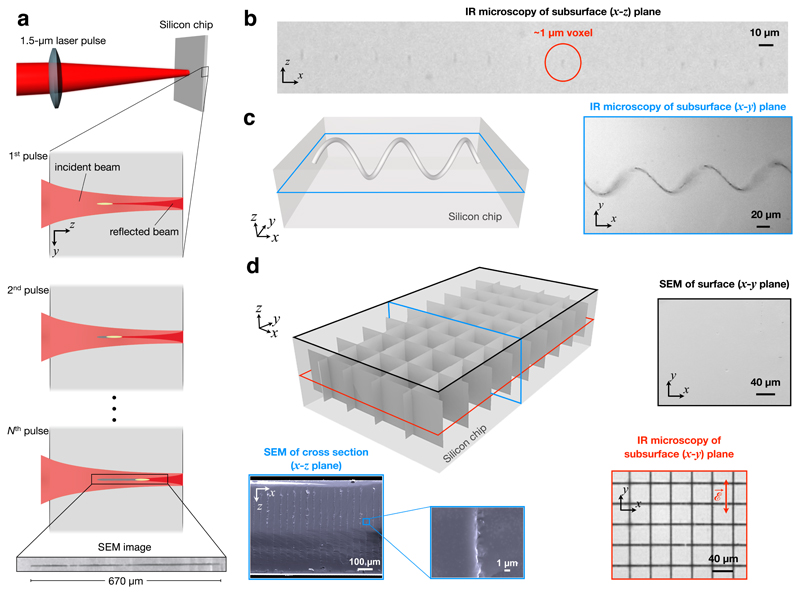
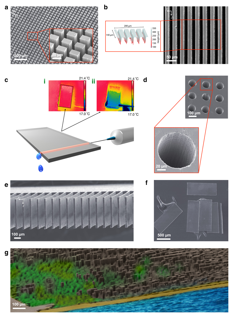
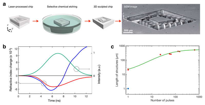
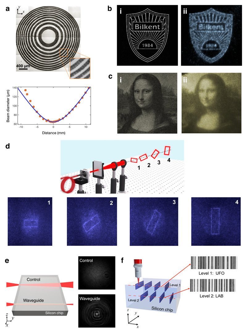
Silicon is an excellent material for microelectronics and integrated photonics1-3 with untapped potential for mid-IR optics4. Despite broad recognition of the importance of the third dimension5,6, current lithography methods do not allow fabrication of photonic devices and functional microelements directly inside silicon chips. Even relatively simple curved geometries cannot be realised with techniques like reactive ion etching. Embedded optical elements, like in glass7, electronic devices, and better electronic-photonic integration are lacking8. Here, we demonstrate laser-based fabrication of complex 3D structures deep inside silicon using 1 µm-sized dots and rod-like structures of adjustable length as basic building blocks. The laser-modified Si has a different optical index than unmodified parts, which enables numerous photonic devices. Optionally, these parts are chemically etched to produce desired 3D shapes. We exemplify a plethora of subsurface, , " microstructures for microfluidic cooling of chips, vias, MEMS, photovoltaic applications and photonic devices that match or surpass the corresponding state-of-the-art device performances.

摘要

硅是微电子和集成光子学的优良材料1-3,在中红外光学领域具有尚未开发的潜力4。尽管人们广泛认识到第三维度5,6的重要性,但目前的光刻方法不允许在硅芯片内部直接制造光子器件和功能性微元件。即使是相对简单的弯曲几何形状也无法通过反应离子蚀刻等技术实现。缺乏像玻璃7、电子器件中那样的嵌入式光学元件以及更好的电子-光子集成8。在这里,我们展示了使用1微米大小的点和长度可调的棒状结构作为基本构建块,在硅内部深处基于激光制造复杂的三维结构。激光改性的硅与未改性部分具有不同的光学折射率,这使得能够制造出众多光子器件。这些部件还可以进行化学蚀刻以产生所需的三维形状。我们举例说明了大量用于芯片微流体冷却、通孔、微机电系统、光伏应用和光子器件的地下“微观结构,这些结构与相应的现有技术器件性能相匹配或超越。

https://cdn.ncbi.nlm.nih.gov/pmc/blobs/6ac4/5624509/039be9579740/emss-73534-f004.jpg
https://cdn.ncbi.nlm.nih.gov/pmc/blobs/6ac4/5624509/b31eb82079ff/emss-73534-f001.jpg
https://cdn.ncbi.nlm.nih.gov/pmc/blobs/6ac4/5624509/4fd649dabe42/emss-73534-f002.jpg
https://cdn.ncbi.nlm.nih.gov/pmc/blobs/6ac4/5624509/1c3edd9c14e9/emss-73534-f003.jpg
https://cdn.ncbi.nlm.nih.gov/pmc/blobs/6ac4/5624509/039be9579740/emss-73534-f004.jpg

相似文献

1
microstructures and photonic devices fabricated by nonlinear laser lithography deep inside silicon.通过非线性激光光刻在硅内部深处制造的微结构和光子器件。
Nat Photonics. 2017 Oct;11(10):639-645. doi: 10.1038/s41566-017-0004-4. Epub 2017 Sep 29.
2
Laser nanofabrication inside silicon with spatial beam modulation and anisotropic seeding.利用空间光束调制和各向异性晶种实现硅内部的激光纳米加工。
Nat Commun. 2024 Jul 16;15(1):5786. doi: 10.1038/s41467-024-49303-z.
3
Controllable Photonic Structures on Silicon-on-Insulator Devices Fabricated Using Femtosecond Laser Lithography.基于飞秒激光光刻技术在绝缘体上硅器件上制备的可控光子结构。
ACS Appl Mater Interfaces. 2021 Sep 15;13(36):43622-43631. doi: 10.1021/acsami.1c11292. Epub 2021 Aug 30.
4
Silica-on-silicon waveguide integrated polydimethylsiloxane lab-on-a-chip for quantum dot fluorescence bio-detection.硅基波导上集成聚二甲基硅氧烷的片上实验室用于量子点荧光生物检测。
J Biomed Opt. 2012 Jan;17(1):017006. doi: 10.1117/1.JBO.17.1.017006.
5
High-Efficiency Multilevel Volume Diffraction Gratings inside Silicon.硅基高效多级体衍射光栅
ACS Mater Au. 2023 Oct 13;3(6):727-733. doi: 10.1021/acsmaterialsau.3c00052. eCollection 2023 Nov 8.
6
Integration of silicon chip microstructures for in-line microbial cell lysis in soft microfluidics.硅芯片微结构的集成用于软微流控中的在线微生物细胞裂解。
Lab Chip. 2023 May 2;23(9):2327-2340. doi: 10.1039/d2lc00896c.
7
Single-chip photonic transceiver based on bulk-silicon, as a chip-level photonic I/O platform for optical interconnects.基于体硅的单芯片光子收发器,作为用于光互连的芯片级光子输入/输出平台。
Sci Rep. 2015 Jun 10;5:11329. doi: 10.1038/srep11329.
8
Robust Microfabrication of Highly Parallelized Three-Dimensional Microfluidics on Silicon.硅基上高度并行化三维微流控的稳健微加工
Sci Rep. 2019 Aug 21;9(1):12213. doi: 10.1038/s41598-019-48515-4.
9
Low-voltage high-performance silicon photonic devices and photonic integrated circuits operating up to 30 Gb/s.工作速率高达30 Gb/s的低压高性能硅光子器件及光子集成电路。
Opt Express. 2011 Dec 19;19(27):26936-47. doi: 10.1364/OE.19.026936.
10
Femtosecond Laser-Fabricated Photonic Chips for Optical Communications: A Review.用于光通信的飞秒激光制造光子芯片:综述
Micromachines (Basel). 2022 Apr 16;13(4):630. doi: 10.3390/mi13040630.

引用本文的文献

1
25 nm-Feature, 10-aspect-ratio, 10 mm-area single-pulsed laser nanolithography.25纳米特征、10纵横比、10平方毫米面积的单脉冲激光纳米光刻技术
Nat Commun. 2025 Aug 12;16(1):7434. doi: 10.1038/s41467-025-62426-1.
2
In-chip critical plasma seeds for laser writing of reconfigurable silicon photonics systems.用于可重构硅光子学系统激光写入的芯片内关键等离子体种子
Nat Commun. 2025 Jul 22;16(1):6733. doi: 10.1038/s41467-025-61983-9.
3
Laser nanofabrication inside silicon with spatial beam modulation and anisotropic seeding.利用空间光束调制和各向异性晶种实现硅内部的激光纳米加工。

本文引用的文献

1
Printing soft matter in three dimensions.三维打印软物质。
Nature. 2016 Dec 14;540(7633):371-378. doi: 10.1038/nature21003.
2
Ablation-cooled material removal with ultrafast bursts of pulses.消融冷却的材料去除与超快脉冲爆发。
Nature. 2016 Sep 1;537(7618):84-88. doi: 10.1038/nature18619. Epub 2016 Jul 13.
3
Multiscale Self-Assembly of Silicon Quantum Dots into an Anisotropic Three-Dimensional Random Network.硅量子点的各向异性三维无规网络的多尺度自组装。
Nat Commun. 2024 Jul 16;15(1):5786. doi: 10.1038/s41467-024-49303-z.
4
Femtosecond Laser Percussion Drilling of Silicon Using Repetitive Single Pulse, MHz-, and GHz-Burst Regimes.使用重复单脉冲、兆赫兹和吉赫兹脉冲序列对硅进行飞秒激光冲击钻孔
Micromachines (Basel). 2024 May 9;15(5):632. doi: 10.3390/mi15050632.
5
Laser manufacturing of spatial resolution approaching quantum limit.空间分辨率接近量子极限的激光制造。
Light Sci Appl. 2024 Jan 2;13(1):6. doi: 10.1038/s41377-023-01354-5.
6
High-Transmission Biomimetics Structural Surfaces Produced via Ultrafast Laser Manufacturing.通过超快激光制造产生的高透射率仿生结构表面
Biomimetics (Basel). 2023 Dec 4;8(8):586. doi: 10.3390/biomimetics8080586.
7
High-Efficiency Multilevel Volume Diffraction Gratings inside Silicon.硅基高效多级体衍射光栅
ACS Mater Au. 2023 Oct 13;3(6):727-733. doi: 10.1021/acsmaterialsau.3c00052. eCollection 2023 Nov 8.
8
Nanoscale multi-beam lithography of photonic crystals with ultrafast laser.利用超快激光对光子晶体进行纳米级多光束光刻。
Light Sci Appl. 2023 Jul 4;12(1):164. doi: 10.1038/s41377-023-01178-3.
9
Impact of film thickness in laser-induced periodic structures on amorphous Si films.激光诱导非晶硅薄膜周期性结构中薄膜厚度的影响。
Front Optoelectron. 2023 Jun 20;16(1):16. doi: 10.1007/s12200-023-00071-6.
10
Comprehensive deep learning model for 3D color holography.用于3D彩色全息术的综合深度学习模型。
Sci Rep. 2022 Feb 15;12(1):2487. doi: 10.1038/s41598-022-06190-y.
Nano Lett. 2016 Mar 9;16(3):1942-8. doi: 10.1021/acs.nanolett.5b05158. Epub 2016 Feb 12.
4
Athermally photoreduced graphene oxides for three-dimensional holographic images.用于三维全息图像的热光还原氧化石墨烯
Nat Commun. 2015 Apr 22;6:6984. doi: 10.1038/ncomms7984.
5
Memory leads the way to better computing.内存引领通往更好计算的道路。
Nat Nanotechnol. 2015 Mar;10(3):191-4. doi: 10.1038/nnano.2015.29.
6
Metasurface holograms reaching 80% efficiency.达到 80%效率的超表面全息图。
Nat Nanotechnol. 2015 Apr;10(4):308-12. doi: 10.1038/nnano.2015.2. Epub 2015 Feb 23.
7
Spectrally selective chiral silicon metasurfaces based on infrared Fano resonances.基于红外 Fano 共振的光谱选择性手性硅超表面。
Nat Commun. 2014 May 27;5:3892. doi: 10.1038/ncomms4892.
8
Diffraction-limited, 10-W, 5-ns, 100-kHz, all-fiber laser at 1.55 μm.波长为1.55μm的衍射极限、10瓦、5纳秒、100千赫兹全光纤激光器。
Opt Lett. 2014 May 1;39(9):2695-8. doi: 10.1364/OL.39.002695.
9
Flat optics with designer metasurfaces.平面光学与设计超表面
Nat Mater. 2014 Feb;13(2):139-50. doi: 10.1038/nmat3839.
10
Silicon nanostructures for photonics and photovoltaics.硅纳米结构用于光子学和光伏技术。
Nat Nanotechnol. 2014 Jan;9(1):19-32. doi: 10.1038/nnano.2013.271.