Hao Lanzhong, Liu Yunjie, Han Zhide, Xu Zhijie, Zhu Jun
College of Science, China University of Petroleum, Qingdao, 266580, Shandong, People's Republic of China.
State Key Laboratory of Electronic Thin Films and Integrated Devices, University of Electronic Science and Technology of China, Chengdu, 610054, People's Republic of China.
Nanoscale Res Lett. 2017 Oct 10;12(1):562. doi: 10.1186/s11671-017-2334-z.
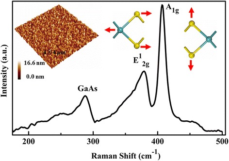
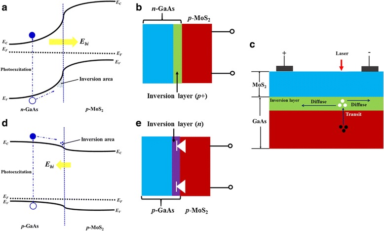
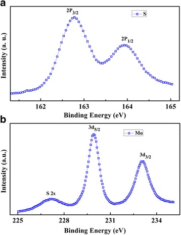
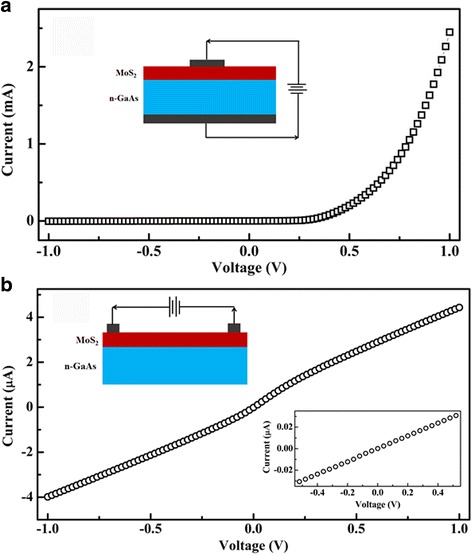
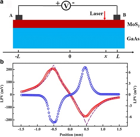
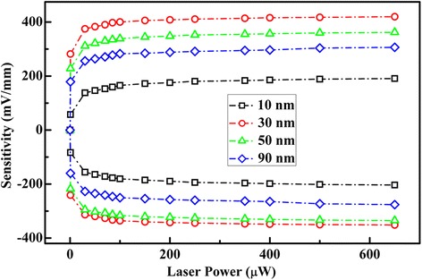
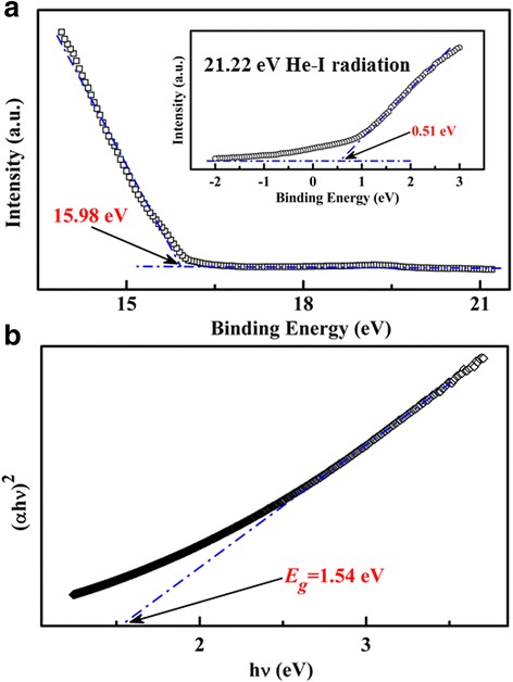
Molybdenum disulfide (MoS) nanoscaled films are deposited on GaAs substrates via magnetron sputtering technique, and MoS/GaAs heterojunctions are fabricated. The lateral photovoltaic effect (LPE) of the fabricated MoS/GaAs heterojunctions is investigated. The results show that a large LPE can be obtained in the MoS/n-GaAs heterojunction. The LPE exhibits a linear dependence on the position of the laser illumination and the considerably high sensitivity of 416.4 mV mm. This sensitivity is much larger than the values in other reported MoS-based devices. Comparatively, the LPE in the MoS/p-GaAs heterojunction is much weaker. The mechanisms to the LPE are unveiled by constructing the energy-band alignment of the MoS/GaAs heterojunctions. The excellent LPE characteristics make MoS films combined with GaAs semiconductors promising candidates for the application of high-performance position-sensitive detectors.
通过磁控溅射技术将二硫化钼(MoS)纳米薄膜沉积在砷化镓(GaAs)衬底上,并制备了MoS/GaAs异质结。对制备的MoS/GaAs异质结的横向光伏效应(LPE)进行了研究。结果表明,在MoS/n-GaAs异质结中可以获得较大的LPE。LPE对激光照射位置呈线性依赖关系,灵敏度高达416.4 mV/mm。该灵敏度远高于其他报道的基于MoS的器件的值。相比之下,MoS/p-GaAs异质结中的LPE要弱得多。通过构建MoS/GaAs异质结的能带排列揭示了LPE的机制。优异的LPE特性使得MoS薄膜与GaAs半导体相结合成为高性能位置敏感探测器应用的有前途的候选材料。