Nakajima H, Morimoto T, Okigawa Y, Yamada T, Ikuta Y, Kawahara K, Ago H, Okazaki T
CNT-Application Research Center, National Institute of Advanced Industrial Science and Technology, Tsukuba 305-8565, Japan.
Nanomaterials Research Institute, National Institute of Advanced Industrial Science and Technology, Tsukuba 305-8565, Japan.
Sci Adv. 2019 Feb 1;5(2):eaau3407. doi: 10.1126/sciadv.aau3407. eCollection 2019 Feb.
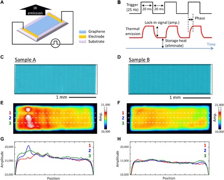
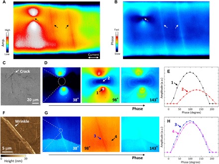
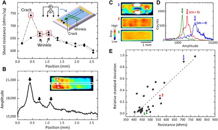
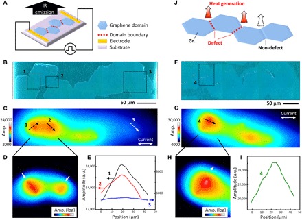
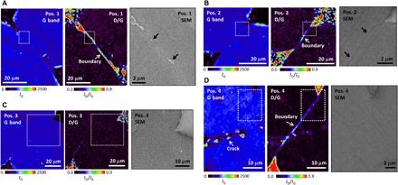
The distribution of defects and dislocations in graphene layers has become a very important concern with regard to the electrical and electronic transport properties of device applications. Although several experiments have shown the influence of defects on the electrical properties of graphene, these studies were limited to measuring microscopic areas because of their long measurement times. Here, we successfully imaged various local defects in a large area of chemical vapor deposition graphene within a reasonable amount of time by using lock-in thermography (LIT). The differences in electrical resistance caused by the micrometer-scale defects, such as cracks and wrinkles, and atomic-scale domain boundaries were apparent as nonuniform Joule heating on polycrystalline and epitaxially grown graphene. The present results indicate that LIT can serve as a fast and effective method of evaluating the quality and uniformity of large graphene films for device applications.
就器件应用的电学和电子输运特性而言,石墨烯层中缺陷和位错的分布已成为一个非常重要的关注点。尽管有几项实验已经表明了缺陷对石墨烯电学性质的影响,但由于测量时间长,这些研究仅限于测量微观区域。在这里,我们通过使用锁相热成像(LIT)在合理的时间内成功地对大面积化学气相沉积石墨烯中的各种局部缺陷进行了成像。由微米级缺陷(如裂纹和皱纹)以及原子级畴界引起的电阻差异,在多晶和外延生长的石墨烯上表现为不均匀的焦耳热。目前的结果表明,LIT可以作为一种快速有效的方法来评估用于器件应用的大型石墨烯薄膜的质量和均匀性。