• 文献检索
  • 文档翻译
  • 深度研究
  • 学术资讯
  • Suppr Zotero 插件Zotero 插件
  • 邀请有礼
  • 套餐&价格
  • 历史记录
应用&插件
Suppr Zotero 插件Zotero 插件浏览器插件Mac 客户端Windows 客户端微信小程序
定价
高级版会员购买积分包购买API积分包
服务
文献检索文档翻译深度研究API 文档MCP 服务
关于我们
关于 Suppr公司介绍联系我们用户协议隐私条款
关注我们

Suppr 超能文献

核心技术专利:CN118964589B侵权必究
粤ICP备2023148730 号-1Suppr @ 2026

文献检索

告别复杂PubMed语法,用中文像聊天一样搜索,搜遍4000万医学文献。AI智能推荐,让科研检索更轻松。

立即免费搜索

文件翻译

保留排版,准确专业,支持PDF/Word/PPT等文件格式,支持 12+语言互译。

免费翻译文档

深度研究

AI帮你快速写综述,25分钟生成高质量综述,智能提取关键信息,辅助科研写作。

立即免费体验

硫族元素空位在二硫化钼中原子缺陷发射方面的作用

The role of chalcogen vacancies for atomic defect emission in MoS.

作者信息

Mitterreiter Elmar, Schuler Bruno, Micevic Ana, Hernangómez-Pérez Daniel, Barthelmi Katja, Cochrane Katherine A, Kiemle Jonas, Sigger Florian, Klein Julian, Wong Edward, Barnard Edward S, Watanabe Kenji, Taniguchi Takashi, Lorke Michael, Jahnke Frank, Finley Johnathan J, Schwartzberg Adam M, Qiu Diana Y, Refaely-Abramson Sivan, Holleitner Alexander W, Weber-Bargioni Alexander, Kastl Christoph

机构信息

Walter Schottky Institut and Physics Department, Technical University of Munich, Garching, Germany.

Munich Center for Quantum Science and Technology (MCQST), München, Germany.

出版信息

Nat Commun. 2021 Jun 22;12(1):3822. doi: 10.1038/s41467-021-24102-y.

DOI:10.1038/s41467-021-24102-y
PMID:34158488
原文链接:https://pmc.ncbi.nlm.nih.gov/articles/PMC8219741/
Abstract

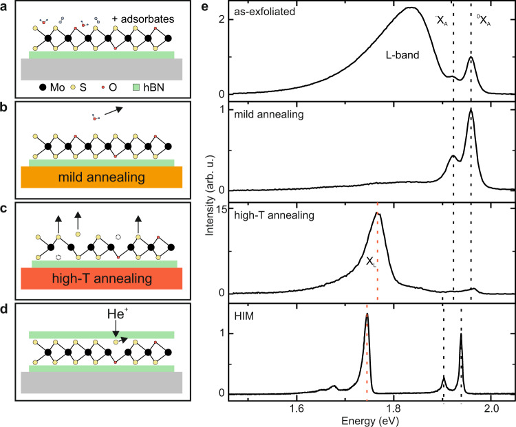
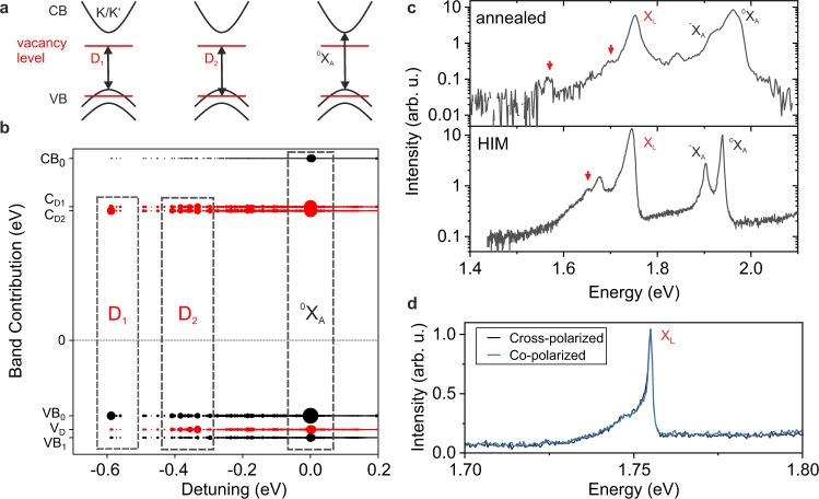
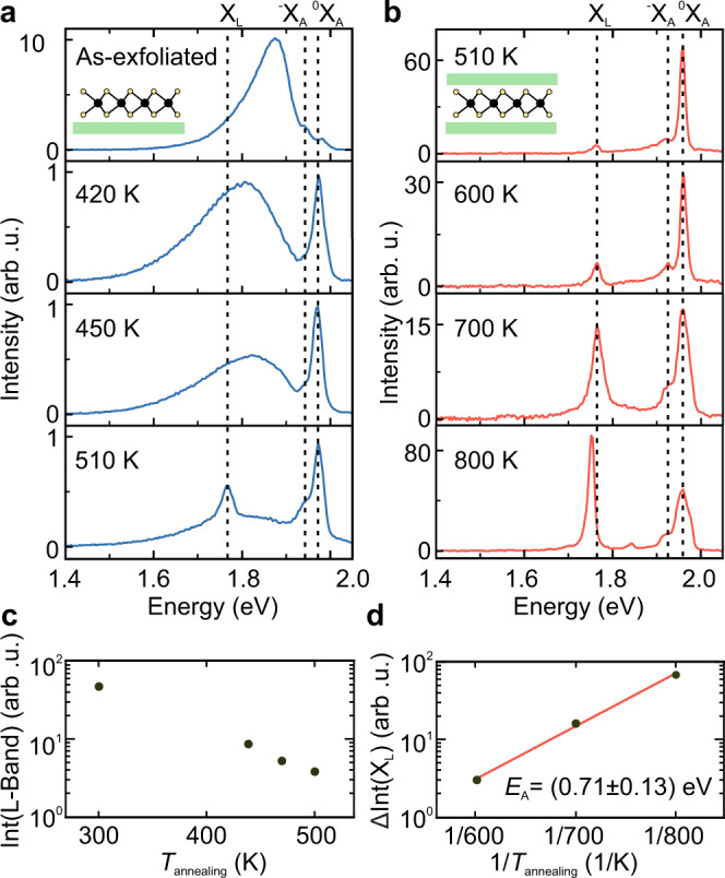
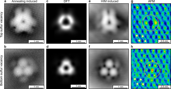
For two-dimensional (2D) layered semiconductors, control over atomic defects and understanding of their electronic and optical functionality represent major challenges towards developing a mature semiconductor technology using such materials. Here, we correlate generation, optical spectroscopy, atomic resolution imaging, and ab initio theory of chalcogen vacancies in monolayer MoS. Chalcogen vacancies are selectively generated by in-vacuo annealing, but also focused ion beam exposure. The defect generation rate, atomic imaging and the optical signatures support this claim. We discriminate the narrow linewidth photoluminescence signatures of vacancies, resulting predominantly from localized defect orbitals, from broad luminescence features in the same spectral range, resulting from adsorbates. Vacancies can be patterned with a precision below 10 nm by ion beams, show single photon emission, and open the possibility for advanced defect engineering of 2D semiconductors at the ultimate scale.

摘要

对于二维(2D)层状半导体而言,控制原子缺陷并理解其电子和光学功能是利用此类材料开发成熟半导体技术面临的主要挑战。在此,我们将单层MoS中硫族元素空位的产生、光谱学、原子分辨率成像和从头算理论关联起来。硫族元素空位可通过真空退火选择性产生,也可通过聚焦离子束曝光产生。缺陷产生率、原子成像和光学特征均支持这一说法。我们区分了空位的窄线宽光致发光特征(主要源于局域缺陷轨道)与同一光谱范围内由吸附物导致的宽发光特征。空位可用离子束以低于10纳米的精度进行图案化,表现出单光子发射,并为二维半导体在极限尺度下的先进缺陷工程开辟了可能性。

https://cdn.ncbi.nlm.nih.gov/pmc/blobs/0e51/8219741/18a0f492cbc9/41467_2021_24102_Fig4_HTML.jpg
https://cdn.ncbi.nlm.nih.gov/pmc/blobs/0e51/8219741/718143594db2/41467_2021_24102_Fig1_HTML.jpg
https://cdn.ncbi.nlm.nih.gov/pmc/blobs/0e51/8219741/12d7f1a66280/41467_2021_24102_Fig2_HTML.jpg
https://cdn.ncbi.nlm.nih.gov/pmc/blobs/0e51/8219741/7433d95f0726/41467_2021_24102_Fig3_HTML.jpg
https://cdn.ncbi.nlm.nih.gov/pmc/blobs/0e51/8219741/18a0f492cbc9/41467_2021_24102_Fig4_HTML.jpg

相似文献

1
The role of chalcogen vacancies for atomic defect emission in MoS.硫族元素空位在二硫化钼中原子缺陷发射方面的作用
Nat Commun. 2021 Jun 22;12(1):3822. doi: 10.1038/s41467-021-24102-y.
2
Room-Temperature Photoluminescence Mediated by Sulfur Vacancies in 2D Molybdenum Disulfide.二维二硫化钼中硫空位介导的室温光致发光
ACS Nano. 2023 Jul 25;17(14):13545-13553. doi: 10.1021/acsnano.3c02103. Epub 2023 Jul 7.
3
Identifying substitutional oxygen as a prolific point defect in monolayer transition metal dichalcogenides.确定替代氧是单层过渡金属二硫属化物中一种常见的点缺陷。
Nat Commun. 2019 Jul 29;10(1):3382. doi: 10.1038/s41467-019-11342-2.
4
Defect evolution behaviors from single sulfur point vacancies to line vacancies in monolayer molybdenum disulfide.单层二硫化钼中从单硫点空位到线空位的缺陷演化行为。
Phys Chem Chem Phys. 2021 Sep 15;23(35):19525-19536. doi: 10.1039/d1cp02852a.
5
Nitrogen Pretreatment of Growth Substrates for Vacancy-Saturated MoS.用于空位饱和MoS₂的生长衬底的氮气预处理
ACS Appl Mater Interfaces. 2023 Sep 13;15(36):42746-42752. doi: 10.1021/acsami.3c07793. Epub 2023 Aug 30.
6
Atomistic Positioning of Defects in Helium Ion Treated Single-Layer MoS.氦离子处理的单层二硫化钼中缺陷的原子定位
Nano Lett. 2020 Jun 10;20(6):4437-4444. doi: 10.1021/acs.nanolett.0c01222. Epub 2020 May 12.
7
MoS Memtransistors Fabricated by Localized Helium Ion Beam Irradiation.通过局部氦离子束辐照制备的金属氧化物半导体场效应晶体管
ACS Nano. 2019 Dec 24;13(12):14262-14273. doi: 10.1021/acsnano.9b07421. Epub 2019 Dec 4.
8
Quantification and Healing of Defects in Atomically Thin Molybdenum Disulfide: Beyond the Controlled Creation of Atomic Defects.原子级薄二硫化钼中缺陷的量化与修复:超越原子缺陷的可控生成
ACS Nano. 2021 Jun 22;15(6):9658-9669. doi: 10.1021/acsnano.0c10897. Epub 2021 Mar 23.
9
Defect Engineering in Single-Layer MoS Using Heavy Ion Irradiation.利用重离子辐照对单层二硫化钼进行缺陷工程
ACS Appl Mater Interfaces. 2018 Dec 12;10(49):42524-42533. doi: 10.1021/acsami.8b17145. Epub 2018 Nov 28.
10
Photovoltage and Photocurrent Absorption Spectra of Sulfur Vacancies Locally Patterned in Monolayer MoS.单层二硫化钼中局部图案化硫空位的光电压和光电流吸收光谱
Nano Lett. 2023 Dec 27;23(24):11655-11661. doi: 10.1021/acs.nanolett.3c03517. Epub 2023 Dec 6.

引用本文的文献

1
Defect identification in monolayer MoTe through tunneling tip-induced charging and theoretical analysis.通过隧穿尖端诱导充电和理论分析识别单层碲化钼中的缺陷
Nanoscale Adv. 2025 Aug 8. doi: 10.1039/d5na00501a.
2
The Effect of Sulfur Vacancy Distribution on Charge Transport across MoS Monolayers: A Quantum Mechanical Study.硫空位分布对电荷跨二硫化钼单层传输的影响:一项量子力学研究。
ACS Mater Au. 2025 Jun 6;5(4):641-655. doi: 10.1021/acsmaterialsau.4c00171. eCollection 2025 Jul 9.
3
Surface-Engineered 2D Nanomaterials in Gas Sensors: Advancement and Challenges.

本文引用的文献

1
Rational Passivation of Sulfur Vacancy Defects in Two-Dimensional Transition Metal Dichalcogenides.二维过渡金属二硫属化物中硫空位缺陷的合理钝化
ACS Nano. 2021 May 25;15(5):8780-8789. doi: 10.1021/acsnano.1c01220. Epub 2021 May 13.
2
Intrinsic donor-bound excitons in ultraclean monolayer semiconductors.超洁净单层半导体中的本征施主束缚激子。
Nat Commun. 2021 Feb 8;12(1):871. doi: 10.1038/s41467-021-21158-8.
3
Gate-Switchable Arrays of Quantum Light Emitters in Contacted Monolayer MoS van der Waals Heterodevices.接触式单层二硫化钼范德华异质结器件中的量子光发射器门控阵列
气体传感器中的表面工程二维纳米材料:进展与挑战
Small. 2025 Aug;21(34):e2410360. doi: 10.1002/smll.202410360. Epub 2025 Jul 4.
4
Graphene-driven correlated electronic states in one dimensional defects within WS.WS₂ 中一维缺陷内的石墨烯驱动的关联电子态
Nat Commun. 2025 Jul 1;16(1):5809. doi: 10.1038/s41467-025-60993-x.
5
Localized exciton emission from monolayer WS nanoribbon at cryogenic temperature.单层 WS 纳米带在低温下的局域激子发射。
Nanophotonics. 2025 Jan 7;14(11):1721-1728. doi: 10.1515/nanoph-2024-0583. eCollection 2025 Jun.
6
Deterministic generation and nanophotonic integration of 2D quantum emitters for advanced quantum photonic functionalities.用于先进量子光子功能的二维量子发射器的确定性生成与纳米光子集成
Nanophotonics. 2025 Jan 24;14(10):1537-1551. doi: 10.1515/nanoph-2024-0629. eCollection 2025 May.
7
Electron Cloaking in MoS for High-Performance Optoelectronics.用于高性能光电器件的二硫化钼中的电子隐身
Nano Lett. 2025 Jun 11;25(23):9463-9469. doi: 10.1021/acs.nanolett.5c02169. Epub 2025 May 28.
8
Subangstrom ion beam engineering of buried ultrathin oxides for scalable quantum computing.用于可扩展量子计算的掩埋超薄氧化物的亚埃离子束工程
Sci Adv. 2025 May 9;11(19):eads9744. doi: 10.1126/sciadv.ads9744. Epub 2025 May 7.
9
Effect of Substrate on Sulfur Vacancy Defect-Mediated Photoluminescence in Two-Dimensional MoS.衬底对二维MoS中硫空位缺陷介导的光致发光的影响
J Phys Chem C Nanomater Interfaces. 2025 Apr 18;129(17):8294-8302. doi: 10.1021/acs.jpcc.4c08491. eCollection 2025 May 1.
10
Giant Light Emission Enhancement in Strain-Engineered InSe/MS (M = Mo or W) van der Waals Heterostructures.应变工程InSe/MS(M = Mo或W)范德华异质结构中的巨光发射增强
Nano Lett. 2025 Mar 5;25(9):3375-3382. doi: 10.1021/acs.nanolett.4c04252. Epub 2025 Feb 5.
Nano Lett. 2021 Jan 27;21(2):1040-1046. doi: 10.1021/acs.nanolett.0c04222. Epub 2021 Jan 12.
4
Exciton-Phonon Interaction and Relaxation Times from First Principles.基于第一性原理的激子-声子相互作用与弛豫时间
Phys Rev Lett. 2020 Sep 4;125(10):107401. doi: 10.1103/PhysRevLett.125.107401.
5
Atomistic Positioning of Defects in Helium Ion Treated Single-Layer MoS.氦离子处理的单层二硫化钼中缺陷的原子定位
Nano Lett. 2020 Jun 10;20(6):4437-4444. doi: 10.1021/acs.nanolett.0c01222. Epub 2020 May 12.
6
Intrinsic and Extrinsic Defect-Related Excitons in TMDCs.过渡金属二硫族化合物中与本征和非本征缺陷相关的激子
Nano Lett. 2020 Apr 8;20(4):2544-2550. doi: 10.1021/acs.nanolett.9b05323. Epub 2020 Mar 24.
7
Filtering the photoluminescence spectra of atomically thin semiconductors with graphene.用石墨烯过滤原子级薄半导体的光致发光光谱。
Nat Nanotechnol. 2020 Apr;15(4):283-288. doi: 10.1038/s41565-020-0644-2. Epub 2020 Mar 9.
8
Large Spin-Orbit Splitting of Deep In-Gap Defect States of Engineered Sulfur Vacancies in Monolayer WS_{2}.单层 WS_{2}中受硫空位工程调制的深能隙内缺陷态的大自旋轨道劈裂
Phys Rev Lett. 2019 Aug 16;123(7):076801. doi: 10.1103/PhysRevLett.123.076801.
9
Identifying substitutional oxygen as a prolific point defect in monolayer transition metal dichalcogenides.确定替代氧是单层过渡金属二硫属化物中一种常见的点缺陷。
Nat Commun. 2019 Jul 29;10(1):3382. doi: 10.1038/s41467-019-11342-2.
10
Site-selectively generated photon emitters in monolayer MoS via local helium ion irradiation.通过局部氦离子辐照在单层二硫化钼中实现位点选择性产生光子发射器。
Nat Commun. 2019 Jun 21;10(1):2755. doi: 10.1038/s41467-019-10632-z.