Quantum Science and Engineering Centre (QSec), Nanyang Technological University, Singapore, 639798, Singapore.
National Key Laboratory of Science and Technology on Micro/Nano Fabrication, Department of Micro/Nano Electronics, Shanghai Jiao Tong University, Shanghai, 200240, China.
Nat Commun. 2022 Feb 24;13(1):1044. doi: 10.1038/s41467-022-28702-0.
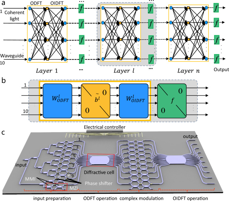
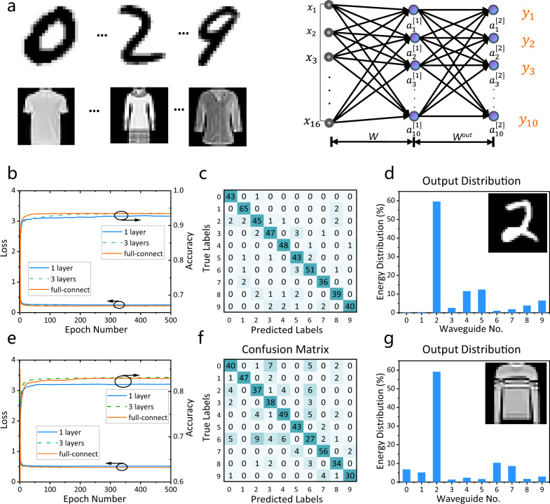
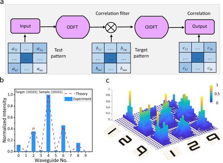
Large-scale, highly integrated and low-power-consuming hardware is becoming progressively more important for realizing optical neural networks (ONNs) capable of advanced optical computing. Traditional experimental implementations need N units such as Mach-Zehnder interferometers (MZIs) for an input dimension N to realize typical computing operations (convolutions and matrix multiplication), resulting in limited scalability and consuming excessive power. Here, we propose the integrated diffractive optical network for implementing parallel Fourier transforms, convolution operations and application-specific optical computing using two ultracompact diffractive cells (Fourier transform operation) and only N MZIs. The footprint and energy consumption scales linearly with the input data dimension, instead of the quadratic scaling in the traditional ONN framework. A ~10-fold reduction in both footprint and energy consumption, as well as equal high accuracy with previous MZI-based ONNs was experimentally achieved for computations performed on the MNIST and Fashion-MNIST datasets. The integrated diffractive optical network (IDNN) chip demonstrates a promising avenue towards scalable and low-power-consumption optical computational chips for optical-artificial-intelligence.
大规模、高度集成和低功耗硬件对于实现能够进行高级光计算的光神经网络 (ONN) 变得越来越重要。传统的实验实现需要 N 个马赫-曾德尔干涉仪 (MZI) 才能实现典型的计算操作(卷积和矩阵乘法),输入维度 N,这导致了有限的可扩展性和过高的功耗。在这里,我们提出了集成衍射光网络,使用两个超紧凑的衍射单元(傅里叶变换操作)和仅 N 个 MZI 来实现并行傅里叶变换、卷积操作和特定于应用的光学计算。足迹和能耗与输入数据维度呈线性关系,而不是传统 ONN 框架中的二次缩放。在 MNIST 和 Fashion-MNIST 数据集上进行计算时,实验实现了约 10 倍的足迹和能耗降低,以及与以前基于 MZI 的 ONN 相等的高精度。集成衍射光网络 (IDNN) 芯片为可扩展和低功耗的光计算芯片开辟了一条有前途的途径,可用于光学人工智能。