• 文献检索
  • 文档翻译
  • 深度研究
  • 学术资讯
  • Suppr Zotero 插件Zotero 插件
  • 邀请有礼
  • 套餐&价格
  • 历史记录
应用&插件
Suppr Zotero 插件Zotero 插件浏览器插件Mac 客户端Windows 客户端微信小程序
定价
高级版会员购买积分包购买API积分包
服务
文献检索文档翻译深度研究API 文档MCP 服务
关于我们
关于 Suppr公司介绍联系我们用户协议隐私条款
关注我们

Suppr 超能文献

核心技术专利:CN118964589B侵权必究
粤ICP备2023148730 号-1Suppr @ 2026

文献检索

告别复杂PubMed语法,用中文像聊天一样搜索,搜遍4000万医学文献。AI智能推荐,让科研检索更轻松。

立即免费搜索

文件翻译

保留排版,准确专业,支持PDF/Word/PPT等文件格式,支持 12+语言互译。

免费翻译文档

深度研究

AI帮你快速写综述,25分钟生成高质量综述,智能提取关键信息,辅助科研写作。

立即免费体验

单晶硅上电沉积硒化镉的优化与表征

Optimization and Characterization of Electrodeposited Cadmium Selenide on Monocrystalline Silicon.

作者信息

Giurlani Walter, Vizza Martina, Leonardi Antonio Alessio, Lo Faro Maria Josè, Irrera Alessia, Innocenti Massimo

机构信息

Dipartimento di Chimica, Università degli Studi di Firenze, Via della Lastruccia 3, 50019 Sesto Fiorentino, Italy.

INSTM, Consorzio Interuniversitario Nazionale per la Scienza e Tecnologia dei Materiali, Via G. Giusti 9, 50121 Firenze, Italy.

出版信息

Nanomaterials (Basel). 2022 Feb 11;12(4):610. doi: 10.3390/nano12040610.

DOI:10.3390/nano12040610
PMID:35214938
原文链接:https://pmc.ncbi.nlm.nih.gov/articles/PMC8875289/
Abstract

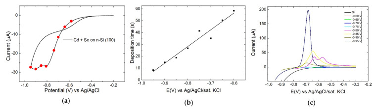
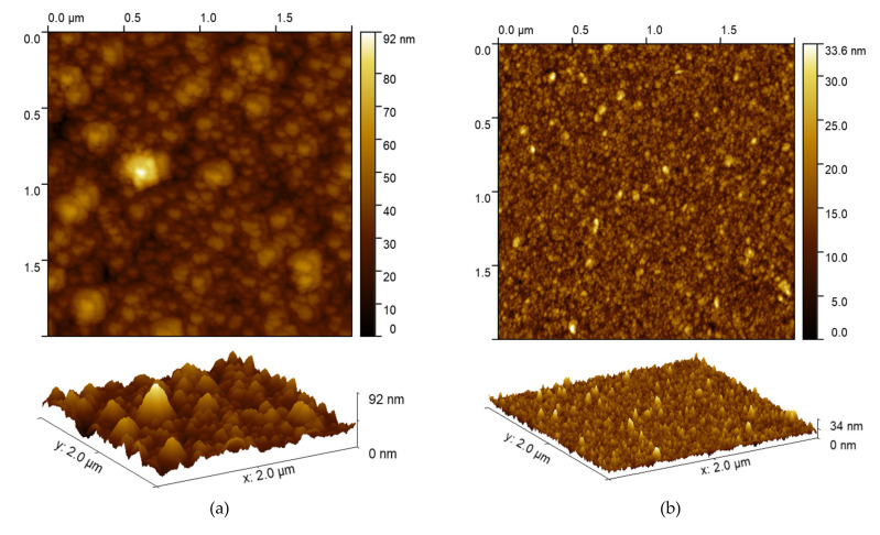
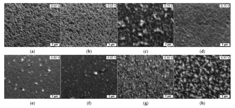
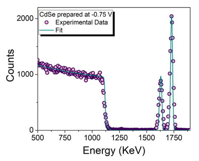
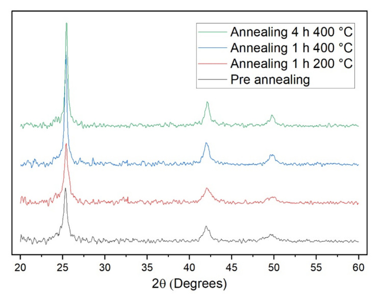
In this work, the optimal conditions for the electrodeposition of a CdSe film on n-Si were demonstrated. The structural and optical properties of the bare films and after annealing were studied. In particular, the crystallinity and photoluminescence of the samples were evaluated, and after annealing at 400 °C under a nitrogen atmosphere, a PL increase by almost an order of magnitude was observed. This paper opens the route towards the use of electrochemical deposition as a cost-effective and easy fabrication approach that can be used to integrate other interesting materials in the silicon-manufacturing processes for the realization of optoelectronic devices.

摘要

在这项工作中,展示了在n型硅上电沉积CdSe薄膜的最佳条件。研究了裸膜及其退火后的结构和光学性质。特别地,评估了样品的结晶度和光致发光,并且在氮气气氛下于400℃退火后,观察到光致发光增加了近一个数量级。本文开启了将电化学沉积作为一种经济高效且易于制造的方法的途径,该方法可用于在硅制造工艺中集成其他有趣的材料以实现光电器件。

https://cdn.ncbi.nlm.nih.gov/pmc/blobs/c167/8875289/af929d211d6e/nanomaterials-12-00610-g005.jpg
https://cdn.ncbi.nlm.nih.gov/pmc/blobs/c167/8875289/524db105ecc6/nanomaterials-12-00610-g001.jpg
https://cdn.ncbi.nlm.nih.gov/pmc/blobs/c167/8875289/7dfcc9a6582e/nanomaterials-12-00610-g002.jpg
https://cdn.ncbi.nlm.nih.gov/pmc/blobs/c167/8875289/306bddda3993/nanomaterials-12-00610-g003.jpg
https://cdn.ncbi.nlm.nih.gov/pmc/blobs/c167/8875289/e4026c851065/nanomaterials-12-00610-g004.jpg
https://cdn.ncbi.nlm.nih.gov/pmc/blobs/c167/8875289/af929d211d6e/nanomaterials-12-00610-g005.jpg

相似文献

1
Optimization and Characterization of Electrodeposited Cadmium Selenide on Monocrystalline Silicon.单晶硅上电沉积硒化镉的优化与表征
Nanomaterials (Basel). 2022 Feb 11;12(4):610. doi: 10.3390/nano12040610.
2
Electrodeposition of Nanoparticles and Continuous Film of CdSe on n-Si (100).在n型硅(100)上进行纳米颗粒和CdSe连续薄膜的电沉积。
Nanomaterials (Basel). 2019 Oct 22;9(10):1504. doi: 10.3390/nano9101504.
3
Rapid thermal evaporation for cadmium selenide thin-film solar cells.用于硒化镉薄膜太阳能电池的快速热蒸发
Front Optoelectron. 2021 Dec;14(4):482-490. doi: 10.1007/s12200-021-1217-1. Epub 2021 May 12.
4
Fabrication of Nanostructured Cadmium Selenide Thin Films for Optoelectronics Applications.用于光电子应用的纳米结构硒化镉薄膜的制备
Front Chem. 2021 Apr 7;9:661723. doi: 10.3389/fchem.2021.661723. eCollection 2021.
5
Exploring the influence of iron doping on structural, morphological and optical properties of chemical bath deposited cadmium selenide thin films for optoelectronic applications.探索铁掺杂对用于光电子应用的化学浴沉积硒化镉薄膜的结构、形态和光学性质的影响。
Heliyon. 2024 Jun 20;10(12):e33311. doi: 10.1016/j.heliyon.2024.e33311. eCollection 2024 Jun 30.
6
Influence of Temperature Reaction for the CdSe-TiO Nanotube Thin Film Formation via Chemical Bath Deposition in Improving the Photoelectrochemical Activity.温度反应对通过化学浴沉积法制备CdSe-TiO纳米管薄膜在提高光电化学活性方面的影响。
Materials (Basel). 2020 Jun 3;13(11):2533. doi: 10.3390/ma13112533.
7
Enhanced Photoluminescence of Hydrogenated Amorphous Silicon Carbide Thin Films by Means of a Fast Thermal Annealing Process.通过快速热退火工艺增强氢化非晶硅碳薄膜的光致发光
Materials (Basel). 2020 Jun 10;13(11):2643. doi: 10.3390/ma13112643.
8
Study of Structural and Optical Properties of Electrodeposited Silicon Films on Graphite Substrates.石墨基底上电沉积硅薄膜的结构与光学性质研究
Nanomaterials (Basel). 2022 Jan 24;12(3):363. doi: 10.3390/nano12030363.
9
[Influence of annealing and sputtering ambience on the photoluminescence of silicon nitride thin films].[退火和溅射气氛对氮化硅薄膜光致发光的影响]
Guang Pu Xue Yu Guang Pu Fen Xi. 2008 Nov;28(11):2494-7.
10
Copper selenide (CuSe and CuSe) thin films: electrochemical deposition and electrocatalytic application in quantum dot-sensitized solar cells.铜硒化物(CuSe 和 CuSe)薄膜:量子点敏化太阳能电池中的电化学沉积和电催化应用。
Dalton Trans. 2018 Nov 27;47(46):16587-16595. doi: 10.1039/c8dt03791d.

引用本文的文献

1
Electrodeposition of Nanostructured Metals on n-Silicon and Insights into Rhodium Deposition.纳米结构金属在n型硅上的电沉积及铑沉积的见解
Nanomaterials (Basel). 2024 Dec 20;14(24):2042. doi: 10.3390/nano14242042.
2
A systematic study of pulse and pulse reverse plating on acid copper bath for decorative and functional applications.对用于装饰和功能性应用的酸性镀铜槽进行脉冲和脉冲反向电镀的系统研究。
Sci Rep. 2022 Oct 28;12(1):18175. doi: 10.1038/s41598-022-22650-x.
3
Electrodeposition of Molybdenum Disulfide (MoS) Nanoparticles on Monocrystalline Silicon.

本文引用的文献

1
Rapid thermal evaporation for cadmium selenide thin-film solar cells.用于硒化镉薄膜太阳能电池的快速热蒸发
Front Optoelectron. 2021 Dec;14(4):482-490. doi: 10.1007/s12200-021-1217-1. Epub 2021 May 12.
2
Erbium emission in Er:YO decorated fractal arrays of silicon nanowires.铒掺杂氧化钇装饰的硅纳米线分形阵列中的铒发射。
Sci Rep. 2020 Jul 30;10(1):12854. doi: 10.1038/s41598-020-69864-5.
3
CMOS-Compatible and Low-Cost Thin Film MACE Approach for Light-Emitting Si NWs Fabrication.用于制造发光硅纳米线的互补金属氧化物半导体兼容且低成本的薄膜金属辅助化学蚀刻方法
二硫化钼(MoS)纳米颗粒在单晶硅上的电沉积
Molecules. 2022 Aug 24;27(17):5416. doi: 10.3390/molecules27175416.
Nanomaterials (Basel). 2020 May 18;10(5):966. doi: 10.3390/nano10050966.
4
Fluorescence Sensor Based on Biosynthetic CdSe/CdS Quantum Dots and Liposome Carrier Signal Amplification for Mercury Detection.基于生物合成 CdSe/CdS 量子点和脂质体载体信号放大的用于汞检测的荧光传感器。
Anal Chem. 2020 Mar 3;92(5):3990-3997. doi: 10.1021/acs.analchem.9b05508. Epub 2020 Feb 14.
5
Electrodeposition of Nanoparticles and Continuous Film of CdSe on n-Si (100).在n型硅(100)上进行纳米颗粒和CdSe连续薄膜的电沉积。
Nanomaterials (Basel). 2019 Oct 22;9(10):1504. doi: 10.3390/nano9101504.
6
Investigations on the Electrochemical Atomic Layer Growth of Bi₂Se₃ and the Surface Limited Deposition of Bismuth at the Silver Electrode.关于Bi₂Se₃的电化学原子层生长及铋在银电极上的表面受限沉积的研究
Materials (Basel). 2018 Aug 14;11(8):1426. doi: 10.3390/ma11081426.
7
Enhanced conversion efficiency in Si solar cells employing photoluminescent down-shifting CdSe/CdS core/shell quantum dots.采用光致发光下转换CdSe/CdS核壳量子点提高硅太阳能电池的转换效率。
Sci Rep. 2017 Oct 26;7(1):14104. doi: 10.1038/s41598-017-14269-0.
8
Effect of core quantum-dot size on power-conversion-efficiency for silicon solar-cells implementing energy-down-shift using CdSe/ZnS core/shell quantum dots.使用CdSe/ZnS核壳量子点实现能量下移的硅太阳能电池中,核心量子点尺寸对功率转换效率的影响。
Nanoscale. 2014 Nov 7;6(21):12524-31. doi: 10.1039/c4nr02472a.
9
Electroluminescent, polycrystalline cadmium selenide nanowire arrays.电致发光、多晶硒化镉纳米线阵列。
ACS Nano. 2013 Oct 22;7(10):9469-79. doi: 10.1021/nn4043546. Epub 2013 Sep 25.
10
Nanoscale evidence of erbium clustering in Er-doped silicon-rich silica.纳米尺度下掺铒硅富石英玻璃中铒原子簇的证据。
Nanoscale Res Lett. 2013 Jan 21;8(1):39. doi: 10.1186/1556-276X-8-39.