Hossain M Khalid, Toki G F Ishraque, Samajdar D P, Mushtaq Muhammad, Rubel M H K, Pandey Rahul, Madan Jaya, Mohammed Mustafa K A, Islam Md Rasidul, Rahman Md Ferdous, Bencherif H
Institute of Electronics, Atomic Energy Research Establishment, Bangladesh Atomic Energy Commission, Dhaka 1349, Bangladesh.
Department of Advanced Energy Engineering Science, Interdisciplinary Graduate School of Engineering Sciences, Kyushu University, Fukuoka 816-8580, Japan.
ACS Omega. 2023 Jun 14;8(25):22466-22485. doi: 10.1021/acsomega.3c00306. eCollection 2023 Jun 27.
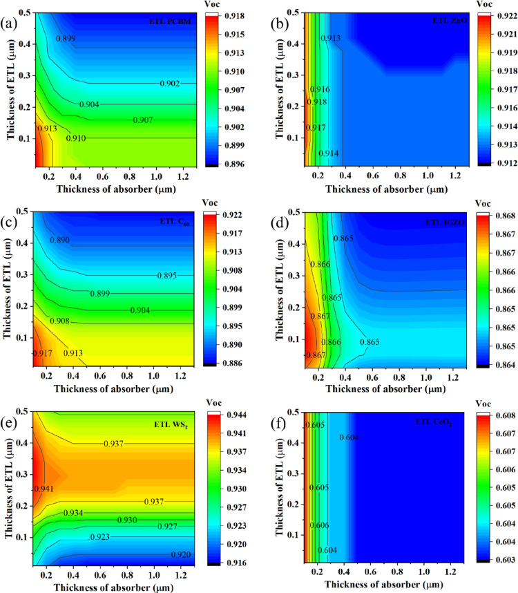
CsSnI is considered to be a viable alternative to lead (Pb)-based perovskite solar cells (PSCs) due to its suitable optoelectronic properties. The photovoltaic (PV) potential of CsSnI has not yet been fully explored due to its inherent difficulties in realizing defect-free device construction owing to the nonoptimized alignment of the electron transport layer (ETL), hole transport layer (HTL), efficient device architecture, and stability issues. In this work, initially, the structural, optical, and electronic properties of the CsSnI perovskite absorber layer were evaluated using the CASTEP program within the framework of the density functional theory (DFT) approach. The band structure analysis revealed that CsSnI is a direct band gap semiconductor with a band gap of 0.95 eV, whose band edges are dominated by Sn 5s/5p electrons After performing the DFT analysis, we investigated the PV performance of a variety of CsSnI-based solar cell configurations utilizing a one-dimensional solar cell capacitance simulator (SCAPS-1D) with different competent ETLs such as IGZO, WS, CeO, TiO, ZnO, PCBM, and C. Simulation results revealed that the device architecture comprising ITO/ETL/CsSnI/CuI/Au exhibited better photoconversion efficiency among more than 70 different configurations. The effect of the variation in the absorber, ETL, and HTL thickness on PV performance was analyzed for the above-mentioned configuration thoroughly. Additionally, the impact of series and shunt resistance, operating temperature, capacitance, Mott-Schottky, generation, and recombination rate on the six superior configurations were evaluated. The - characteristics and the quantum efficiency plots for these devices are systematically investigated for in-depth analysis. Consequently, this extensive simulation with validation results established the true potential of CsSnI absorber with suitable ETLs including ZnO, IGZO, WS, PCBM, CeO, and C ETLs and CuI as HTL, paving a constructive research path for the photovoltaic industry to fabricate cost-effective, high-efficiency, and nontoxic CsSnI PSCs.
由于其合适的光电特性,CsSnI被认为是基于铅(Pb)的钙钛矿太阳能电池(PSC)的可行替代品。由于在实现无缺陷器件结构方面存在固有困难,如电子传输层(ETL)、空穴传输层(HTL)的非优化排列、高效的器件结构以及稳定性问题,CsSnI的光伏(PV)潜力尚未得到充分探索。在这项工作中,首先,在密度泛函理论(DFT)方法的框架内,使用CASTEP程序评估了CsSnI钙钛矿吸收层的结构、光学和电子性质。能带结构分析表明,CsSnI是一种直接带隙半导体,带隙为0.95 eV,其能带边缘由Sn 5s/5p电子主导。在进行DFT分析后,我们利用一维太阳能电池电容模拟器(SCAPS-1D)研究了各种基于CsSnI的太阳能电池配置的光伏性能,这些配置使用了不同的有竞争力的ETL,如IGZO、WS、CeO、TiO、ZnO、PCBM和C。模拟结果表明,在70多种不同配置中,由ITO/ETL/CsSnI/CuI/Au组成的器件结构表现出更好的光电转换效率。针对上述配置,深入分析了吸收层、ETL和HTL厚度变化对光伏性能的影响。此外,还评估了串联和并联电阻、工作温度、电容、莫特-肖特基效应、产生和复合率对六种优异配置的影响。系统地研究了这些器件的I-V特性和量子效率图,以进行深入分析。因此,这项具有验证结果的广泛模拟确定了CsSnI吸收层与包括ZnO、IGZO、WS、PCBM、CeO和C ETL以及CuI作为HTL的合适ETL相结合的真正潜力,为光伏产业制造具有成本效益、高效且无毒的CsSnI PSC铺平了建设性的研究道路。