Liu Xia, Erbas Berke, Conde-Rubio Ana, Rivano Norma, Wang Zhenyu, Jiang Jin, Bienz Siiri, Kumar Naresh, Sohier Thibault, Penedo Marcos, Banerjee Mitali, Fantner Georg, Zenobi Renato, Marzari Nicola, Kis Andras, Boero Giovanni, Brugger Juergen
Microsystems Laboratory, École Polytechnique Fédérale de Lausanne (EPFL), 1015, Lausanne, Switzerland.
School of Integrated Circuits and Electronics, MIIT Key Laboratory for Low-Dimensional Quantum Structure and Devices, Beijing Institute of Technology, Beijing, 100081, China.
Nat Commun. 2024 Aug 13;15(1):6934. doi: 10.1038/s41467-024-51165-4.
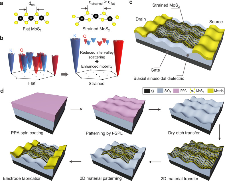
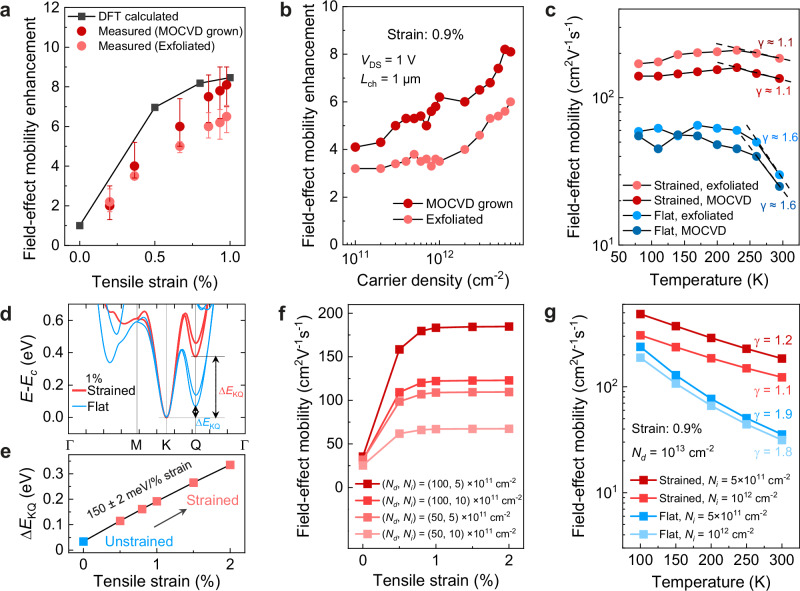
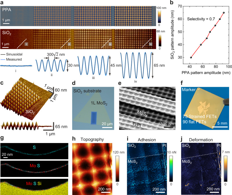
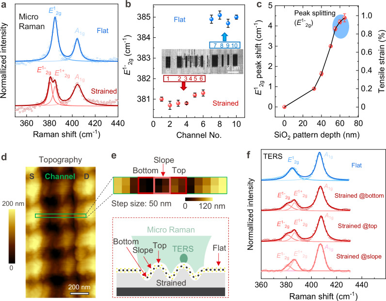
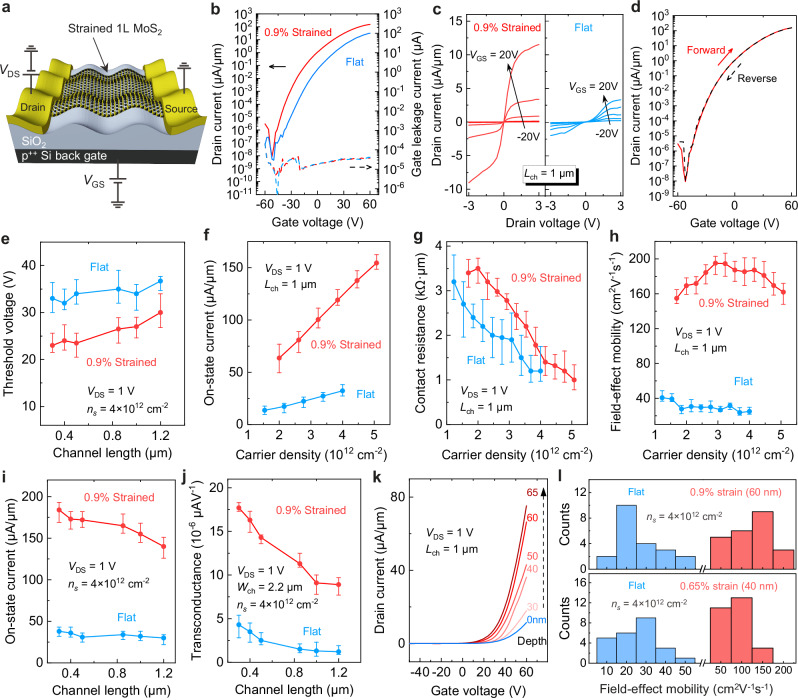
Field-effect transistors (FETs) based on two-dimensional materials (2DMs) with atomically thin channels have emerged as a promising platform for beyond-silicon electronics. However, low carrier mobility in 2DM transistors driven by phonon scattering remains a critical challenge. To address this issue, we propose the controlled introduction of localized tensile strain as an effective means to inhibit electron-phonon scattering in 2DM. Strain is achieved by conformally adhering the 2DM via van der Waals forces to a dielectric layer previously nanoengineered with a gray-tone topography. Our results show that monolayer MoS FETs under tensile strain achieve an 8-fold increase in on-state current, reaching mobilities of 185 cm²/Vs at room temperature, in good agreement with theoretical calculations. The present work on nanotopographic grayscale surface engineering and the use of high-quality dielectric materials has the potential to find application in the nanofabrication of photonic and nanoelectronic devices.
基于具有原子级薄通道的二维材料(2DM)的场效应晶体管(FET)已成为超越硅电子学的一个有前景的平台。然而,由声子散射驱动的2DM晶体管中低载流子迁移率仍然是一个关键挑战。为了解决这个问题,我们提出可控引入局部拉伸应变作为抑制2DM中电子 - 声子散射的有效手段。通过范德华力将2DM共形粘附到先前用灰度形貌进行纳米工程处理的介电层上来实现应变。我们的结果表明,处于拉伸应变下的单层MoS FET的导通态电流增加了8倍,在室温下迁移率达到185 cm²/Vs,与理论计算结果高度吻合。目前关于纳米形貌灰度表面工程以及高质量介电材料的应用,有潜力在光子和纳米电子器件的纳米制造中得到应用。