Lee Jeong-Min, Lee Seo-Hyun, Lee Ji Hun, Kwak Junghun, Lee Jinhee, Kim Woo-Hee
Department of Materials Science and Chemical Engineering, BK21 FOUR ERICA-ACE Center, Hanyang University, Ansan, Gyeonggi, 15588, Republic of Korea.
SK Specialty Co., Ltd, 59-33 Gaheunggongdan-ro, Yeongju-Si, Gyeongsangbuk-Do, 36059, Korea.
Nano Converg. 2025 May 30;12(1):27. doi: 10.1186/s40580-025-00490-5.
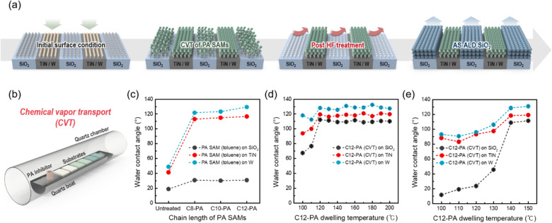
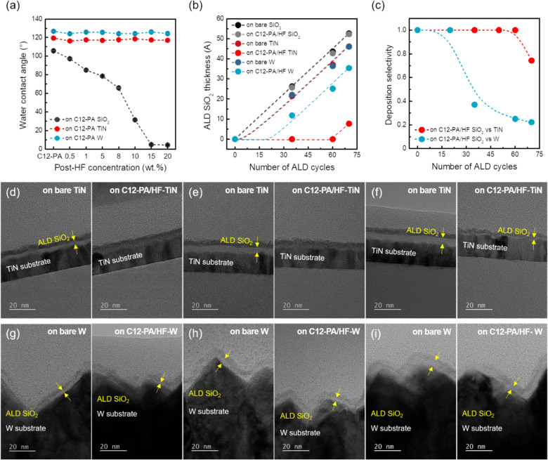
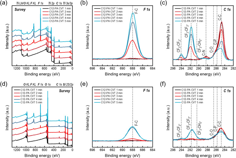
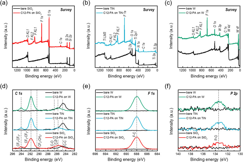
Aiming for atomic-scale precision alignment for advanced semiconductor devices, area-selective atomic layer deposition (AS-ALD) has garnered substantial attention because of its bottom-up nature that allows precise control of material deposition exclusively on desired areas. In this study, we develop a surface treatment to hinder the adsorption of Si precursor on metal surfaces by using a vapor-phase functionalization of bulky phosphonic acid (PA) self-assembled monolayers (SAMs). Through the chemical vapor transport (CVT) method, the bulky solid PA inhibitor with a fluorocarbon terminal group was effectively vaporized, and the conditions for maximizing the blocking effect of the inhibitor were confirmed by optimizing the process temperature and dwelling time. The unintended PA inhibitors adsorbed on SiO surfaces during the CVT process were selectively removed by post-HF treatment, thereby leading to selective deposition of SiO thin films only on SiO substrates. As a results, SiO film growth on the PA SAM/HF-treated TiN surfaces was suppressed by up to 4 nm with just a single exposure to the long-chain inhibitor, even during the ALD process using highly reactive O reactants. The proposed approach paves the way for highly selective deposition of dielectrics on dielectrics (DoD).
为了实现先进半导体器件的原子尺度精确对准,区域选择性原子层沉积(AS-ALD)因其自下而上的特性而备受关注,该特性允许仅在所需区域精确控制材料沉积。在本研究中,我们通过使用大体积膦酸(PA)自组装单分子层(SAMs)的气相功能化来开发一种表面处理方法,以阻碍Si前驱体在金属表面的吸附。通过化学气相传输(CVT)方法,有效地蒸发了具有氟碳端基的大体积固体PA抑制剂,并通过优化工艺温度和停留时间确定了使抑制剂的阻断效果最大化的条件。在CVT过程中吸附在SiO表面上的意外PA抑制剂通过后HF处理被选择性去除,从而仅在SiO衬底上导致SiO薄膜的选择性沉积。结果,即使在使用高反应性O反应物的ALD过程中,仅单次暴露于长链抑制剂,PA SAM/HF处理的TiN表面上的SiO膜生长就被抑制了多达4nm。所提出的方法为在电介质上进行高选择性电介质沉积(DoD)铺平了道路。