• 文献检索
  • 文档翻译
  • 深度研究
  • 学术资讯
  • Suppr Zotero 插件Zotero 插件
  • 邀请有礼
  • 套餐&价格
  • 历史记录
应用&插件
Suppr Zotero 插件Zotero 插件浏览器插件Mac 客户端Windows 客户端微信小程序
定价
高级版会员购买积分包购买API积分包
服务
文献检索文档翻译深度研究API 文档MCP 服务
关于我们
关于 Suppr公司介绍联系我们用户协议隐私条款
关注我们

Suppr 超能文献

核心技术专利:CN118964589B侵权必究
粤ICP备2023148730 号-1Suppr @ 2026

文献检索

告别复杂PubMed语法,用中文像聊天一样搜索,搜遍4000万医学文献。AI智能推荐,让科研检索更轻松。

立即免费搜索

文件翻译

保留排版,准确专业,支持PDF/Word/PPT等文件格式,支持 12+语言互译。

免费翻译文档

深度研究

AI帮你快速写综述,25分钟生成高质量综述,智能提取关键信息,辅助科研写作。

立即免费体验

亚 10 纳米栅长石墨烯晶体管:在太赫兹频率下实现电流饱和工作。

Sub-10 nm gate length graphene transistors: operating at terahertz frequencies with current saturation.

机构信息

State Key Laboratory of Mesoscopic Physics and Department of Physics, Peking University, Beijing 100871, P. R. China.

出版信息

Sci Rep. 2013;3:1314. doi: 10.1038/srep01314.

DOI:10.1038/srep01314
PMID:23419782
原文链接:https://pmc.ncbi.nlm.nih.gov/articles/PMC3575621/
Abstract

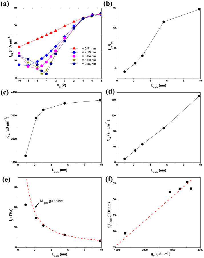
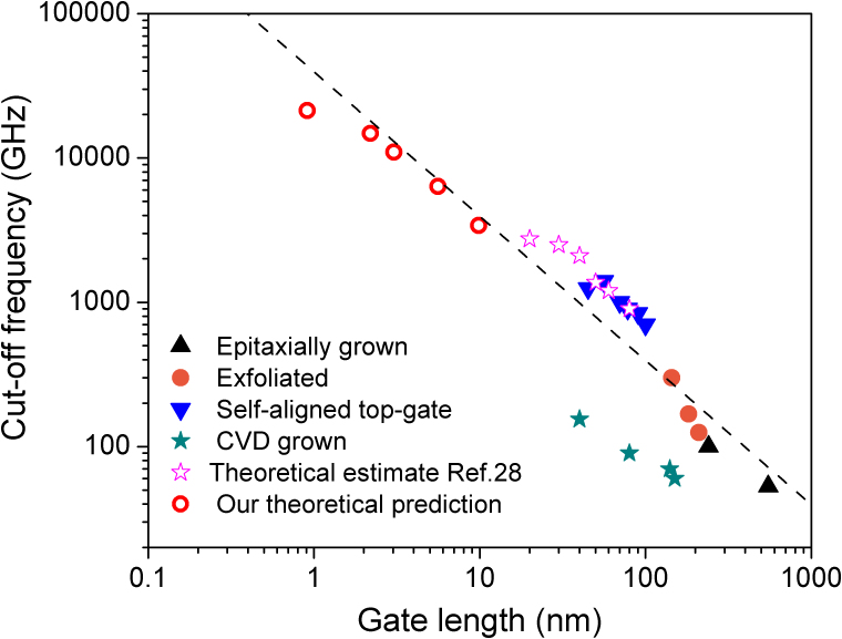
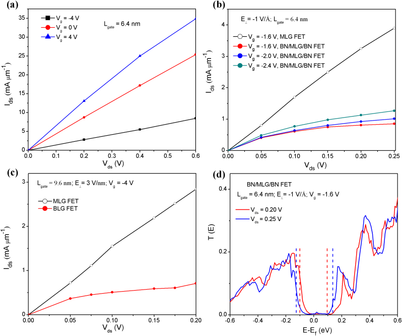
Radio-frequency application of graphene transistors is attracting much recent attention due to the high carrier mobility of graphene. The measured intrinsic cut-off frequency (f(T)) of graphene transistor generally increases with the reduced gate length (L(gate)) till L(gate) = 40 nm, and the maximum measured f(T) has reached 300 GHz. Using ab initio quantum transport simulation, we reveal for the first time that f(T) of a graphene transistor still increases with the reduced L(gate) when L(gate) scales down to a few nm and reaches astonishing a few tens of THz. We observe a clear drain current saturation when a band gap is opened in graphene, with the maximum intrinsic voltage gain increased by a factor of 20. Our simulation strongly suggests it is possible to design a graphene transistor with an extraordinary high f(T) and drain current saturation by continuously shortening L(gate) and opening a band gap.

摘要

由于石墨烯具有较高的载流子迁移率,因此其晶体管的射频应用近来受到了广泛关注。通过测量,石墨烯晶体管的本征截止频率(f(T))通常随着栅长(L(gate))的减小而增大,直至 L(gate) = 40nm,最大测量 f(T) 已达到 300GHz。通过使用从头算量子输运模拟,我们首次揭示了当栅长缩小到几纳米时,石墨烯晶体管的 f(T) 仍随着栅长的减小而增大,并达到惊人的几十太赫兹。当石墨烯中出现带隙时,我们观察到漏电流明显饱和,最大本征电压增益增加了 20 倍。我们的模拟强烈表明,通过不断缩短 L(gate)并打开带隙,设计具有超高 f(T)和漏电流饱和的石墨烯晶体管是有可能的。

https://cdn.ncbi.nlm.nih.gov/pmc/blobs/c155/3575621/b9bb431b6d77/srep01314-f7.jpg
https://cdn.ncbi.nlm.nih.gov/pmc/blobs/c155/3575621/42750bb03915/srep01314-f1.jpg
https://cdn.ncbi.nlm.nih.gov/pmc/blobs/c155/3575621/fd7ed034c1ab/srep01314-f2.jpg
https://cdn.ncbi.nlm.nih.gov/pmc/blobs/c155/3575621/3dfc19bffe6b/srep01314-f3.jpg
https://cdn.ncbi.nlm.nih.gov/pmc/blobs/c155/3575621/b9980e9178cc/srep01314-f4.jpg
https://cdn.ncbi.nlm.nih.gov/pmc/blobs/c155/3575621/3e8c6f6be62a/srep01314-f5.jpg
https://cdn.ncbi.nlm.nih.gov/pmc/blobs/c155/3575621/335ab2cfc0a6/srep01314-f6.jpg
https://cdn.ncbi.nlm.nih.gov/pmc/blobs/c155/3575621/b9bb431b6d77/srep01314-f7.jpg

相似文献

1
Sub-10 nm gate length graphene transistors: operating at terahertz frequencies with current saturation.亚 10 纳米栅长石墨烯晶体管:在太赫兹频率下实现电流饱和工作。
Sci Rep. 2013;3:1314. doi: 10.1038/srep01314.
2
High-speed graphene transistors with a self-aligned nanowire gate.具有自对准纳米线栅的高速石墨烯晶体管。
Nature. 2010 Sep 16;467(7313):305-8. doi: 10.1038/nature09405. Epub 2010 Sep 1.
3
High-frequency graphene voltage amplifier.高频石墨烯电压放大器。
Nano Lett. 2011 Sep 14;11(9):3690-3. doi: 10.1021/nl2016637. Epub 2011 Aug 5.
4
Sub-100 nm channel length graphene transistors.亚 100nm 沟道长度石墨烯晶体管。
Nano Lett. 2010 Oct 13;10(10):3952-6. doi: 10.1021/nl101724k.
5
Growth of graphene with large single-crystal domains by Ni foam-assisted structure and its high-gain field-effect transistors.泡沫镍辅助结构制备具有大单晶晶畴的石墨烯及其高增益场效应晶体管
Nanoscale Adv. 2018 Dec 13;1(3):1130-1135. doi: 10.1039/c8na00203g. eCollection 2019 Mar 12.
6
High-frequency, scaled graphene transistors on diamond-like carbon.在类金刚石碳上的高频、可扩展的石墨烯晶体管。
Nature. 2011 Apr 7;472(7341):74-8. doi: 10.1038/nature09979.
7
High-frequency self-aligned graphene transistors with transferred gate stacks.具有转移栅堆叠的高频自对准石墨烯晶体管。
Proc Natl Acad Sci U S A. 2012 Jul 17;109(29):11588-92. doi: 10.1073/pnas.1205696109. Epub 2012 Jul 2.
8
Current saturation in submicrometer graphene transistors with thin gate dielectric: experiment, simulation, and theory.亚微米栅介质下石墨烯晶体管中的电流饱和:实验、模拟与理论。
ACS Nano. 2012 Jun 26;6(6):5220-6. doi: 10.1021/nn300978c. Epub 2012 May 21.
9
200 GHz Maximum Oscillation Frequency in CVD Graphene Radio Frequency Transistors.CVD 石墨烯射频晶体管中 200GHz 的最大振荡频率。
ACS Appl Mater Interfaces. 2016 Oct 5;8(39):25645-25649. doi: 10.1021/acsami.6b05791. Epub 2016 Sep 26.
10
Operation of graphene transistors at gigahertz frequencies.石墨烯晶体管在千兆赫频率下的运行。
Nano Lett. 2009 Jan;9(1):422-6. doi: 10.1021/nl803316h.

引用本文的文献

1
Novel graphene-like two-dimensional bilayer germanene dioxide: electronic structure and optical properties.新型类石墨烯二维双层二氧化锗:电子结构与光学性质
RSC Adv. 2019 Mar 27;9(17):9633-9639. doi: 10.1039/c9ra00450e. eCollection 2019 Mar 22.
2
Freestanding Graphene Fabric Film for Flexible Infrared Camouflage.用于柔性红外伪装的独立式石墨烯织物薄膜
Adv Sci (Weinh). 2022 Feb;9(5):e2105004. doi: 10.1002/advs.202105004. Epub 2021 Dec 16.
3
Noise and charge discreteness as ultimate limit for the THz operation of ultra-small electronic devices.

本文引用的文献

1
Current saturation and voltage gain in bilayer graphene field effect transistors.双层石墨烯场效应晶体管中的电流饱和和电压增益。
Nano Lett. 2012 Mar 14;12(3):1324-8. doi: 10.1021/nl2038634. Epub 2012 Feb 22.
2
Quantum behavior of graphene transistors near the scaling limit.石墨烯晶体管在接近缩放极限时的量子行为。
Nano Lett. 2012 Mar 14;12(3):1417-23. doi: 10.1021/nl204088b. Epub 2012 Feb 15.
3
Field-effect tunneling transistor based on vertical graphene heterostructures.基于垂直石墨烯异质结构的场效应隧穿晶体管。
噪声和电荷离散性是超小型电子器件太赫兹运行的最终限制。
Sci Rep. 2020 Oct 2;10(1):15990. doi: 10.1038/s41598-020-72982-9.
4
Camphor-Based CVD Bilayer Graphene/Si Heterostructures for Self-Powered and Broadband Photodetection.用于自供电宽带光电探测的樟脑基化学气相沉积双层石墨烯/硅异质结构
Micromachines (Basel). 2020 Aug 27;11(9):812. doi: 10.3390/mi11090812.
5
How Important Is the Metal-Semiconductor Contact for Schottky Barrier Transistors: A Case Study on Few-Layer Black Phosphorus?肖特基势垒晶体管中的金属-半导体接触有多重要:以少层黑磷为例的研究?
ACS Omega. 2017 Aug 3;2(8):4173-4179. doi: 10.1021/acsomega.7b00634. eCollection 2017 Aug 31.
6
Tunable Electronic and Topological Properties of Germanene by Functional Group Modification.通过官能团修饰调控锗烯的电子和拓扑性质
Nanomaterials (Basel). 2018 Mar 6;8(3):145. doi: 10.3390/nano8030145.
7
The Growth Mechanism of Transition Metal Dichalcogenides by using Sulfurization of Pre-deposited Transition Metals and the 2D Crystal Hetero-structure Establishment.通过预沉积过渡金属的硫化和二维晶体异质结构的建立来研究过渡金属二硫属化物的生长机制。
Sci Rep. 2017 Feb 8;7:42146. doi: 10.1038/srep42146.
8
Deep-submicron Graphene Field-Effect Transistors with State-of-Art f.具有先进截止频率的深亚微米石墨烯场效应晶体管
Sci Rep. 2016 Oct 24;6:35717. doi: 10.1038/srep35717.
9
Graphene mobility mapping.石墨烯迁移率测绘
Sci Rep. 2015 Jul 24;5:12305. doi: 10.1038/srep12305.
10
Silicene nanomesh.硅烯纳米网
Sci Rep. 2015 Mar 13;5:9075. doi: 10.1038/srep09075.
Science. 2012 Feb 24;335(6071):947-50. doi: 10.1126/science.1218461. Epub 2012 Feb 2.
4
Sub-10 nm carbon nanotube transistor.亚 10nm 碳纳米管晶体管。
Nano Lett. 2012 Feb 8;12(2):758-62. doi: 10.1021/nl203701g. Epub 2012 Jan 18.
5
A role for graphene in silicon-based semiconductor devices.石墨烯在硅基半导体器件中的作用。
Nature. 2011 Nov 16;479(7373):338-44. doi: 10.1038/nature10680.
6
Tunable bandgap in silicene and germanene.硅烯和锗烯中的可调带隙。
Nano Lett. 2012 Jan 11;12(1):113-8. doi: 10.1021/nl203065e. Epub 2011 Dec 21.
7
Mapping the density of scattering centers limiting the electron mean free path in graphene.绘制限制石墨烯中电子平均自由程的散射中心密度图。
Nano Lett. 2011 Nov 9;11(11):4612-8. doi: 10.1021/nl2020922. Epub 2011 Oct 12.
8
Scalable fabrication of self-aligned graphene transistors and circuits on glass.在玻璃上可扩展制造自对准石墨烯晶体管和电路。
Nano Lett. 2012 Jun 13;12(6):2653-7. doi: 10.1021/nl201922c. Epub 2011 Jun 14.
9
Micrometer-scale ballistic transport in encapsulated graphene at room temperature.室温下封装石墨烯中的微米级弹道输运。
Nano Lett. 2011 Jun 8;11(6):2396-9. doi: 10.1021/nl200758b. Epub 2011 May 16.
10
Top-gated chemical vapor deposition grown graphene transistors with current saturation.顶栅式化学气相沉积生长的具有电流饱和特性的石墨烯晶体管。
Nano Lett. 2011 Jun 8;11(6):2555-9. doi: 10.1021/nl201331x. Epub 2011 May 6.