Lin Hung-Cheng, Stehlin Fabrice, Soppera Olivier, Zan Hsiao-Wen, Li Chang-Hung, Wieder Fernand, Ponche Arnaud, Berling Dominique, Yeh Bo-Hung, Wang Kuan-Hsun
Department of Photonics and Institute of Electro-Optics, National Chiao Tung University, 1001 Ta Hsueh Rd., 300 HsinChu, Taiwan.
Institut de Science des Matériaux de Mulhouse (IS2M), CNRS - UMR 7361, Université de Haute Alsace, 15 rue Jean Starcky, Mulhouse, France.
Sci Rep. 2015 May 27;5:10490. doi: 10.1038/srep10490.
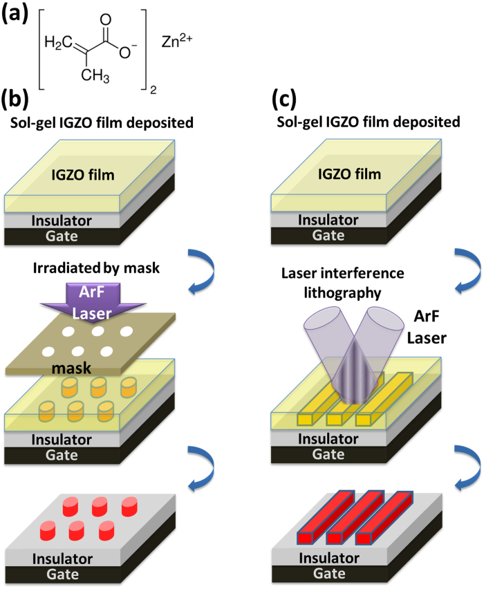
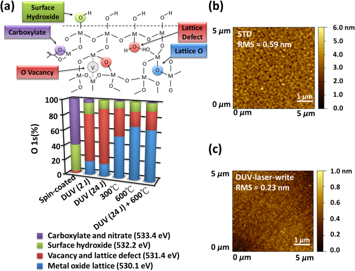
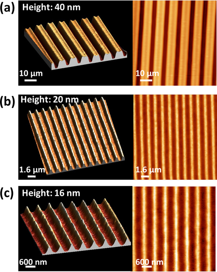
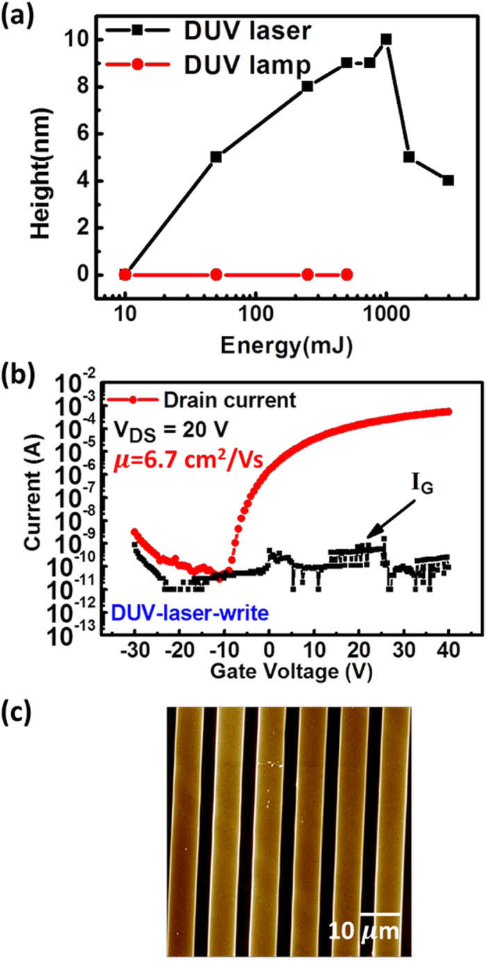
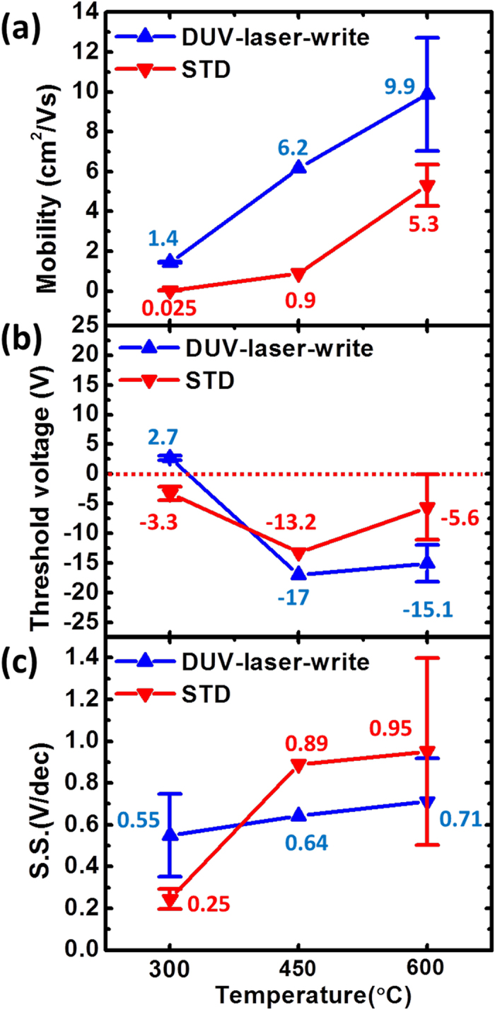
Deep-UV (DUV) laser was used to directly write indium-gallium-zinc-oxide (IGZO) precursor solution and form micro and nanoscale patterns. The directional DUV laser beam avoids the substrate heating and suppresses the diffraction effect. A IGZO precursor solution was also developed to fulfill the requirements for direct photopatterning and for achieving semi-conducting properties with thermal annealing at moderate temperature. The DUV-induced crosslinking of the starting material allows direct write of semi-conducting channels in thin-film transistors but also it improves the field-effect mobility and surface roughness. Material analysis has been carried out by XPS, FTIR, spectroscopic ellipsometry and AFM and the effect of DUV on the final material structure is discussed. The DUV irradiation step results in photolysis and a partial condensation of the inorganic network that freezes the sol-gel layer in a homogeneous distribution, lowering possibilities of thermally induced reorganization at the atomic scale. Laser irradiation allows high-resolution photopatterning and high-enough field-effect mobility, which enables the easy fabrication of oxide nanowires for applications in solar cell, display, flexible electronics, and biomedical sensors.
深紫外(DUV)激光用于直接写入铟镓锌氧化物(IGZO)前驱体溶液并形成微米和纳米级图案。定向DUV激光束可避免基板受热并抑制衍射效应。还开发了一种IGZO前驱体溶液,以满足直接光图案化以及通过在适度温度下进行热退火实现半导体性能的要求。起始材料的DUV诱导交联不仅允许在薄膜晶体管中直接写入半导体通道,还提高了场效应迁移率和表面粗糙度。通过XPS、FTIR、光谱椭偏仪和AFM进行了材料分析,并讨论了DUV对最终材料结构的影响。DUV辐照步骤导致光解和无机网络的部分缩合,从而使溶胶-凝胶层以均匀分布冻结,降低了原子尺度上热诱导重组的可能性。激光辐照允许进行高分辨率光图案化以及足够高的场效应迁移率,这使得能够轻松制造用于太阳能电池、显示器、柔性电子和生物医学传感器的氧化物纳米线。