• 文献检索
  • 文档翻译
  • 深度研究
  • 学术资讯
  • Suppr Zotero 插件Zotero 插件
  • 邀请有礼
  • 套餐&价格
  • 历史记录
应用&插件
Suppr Zotero 插件Zotero 插件浏览器插件Mac 客户端Windows 客户端微信小程序
定价
高级版会员购买积分包购买API积分包
服务
文献检索文档翻译深度研究API 文档MCP 服务
关于我们
关于 Suppr公司介绍联系我们用户协议隐私条款
关注我们

Suppr 超能文献

核心技术专利:CN118964589B侵权必究
粤ICP备2023148730 号-1Suppr @ 2026

文献检索

告别复杂PubMed语法,用中文像聊天一样搜索,搜遍4000万医学文献。AI智能推荐,让科研检索更轻松。

立即免费搜索

文件翻译

保留排版,准确专业,支持PDF/Word/PPT等文件格式,支持 12+语言互译。

免费翻译文档

深度研究

AI帮你快速写综述,25分钟生成高质量综述,智能提取关键信息,辅助科研写作。

立即免费体验

一种用于制造砷化铟纳米线场效应晶体管的软光刻方法。

A soft lithographic approach to fabricate InAs nanowire field-effect transistors.

作者信息

Lee Sang Hwa, Shin Sung-Ho, Madsen Morten, Takei Kuniharu, Nah Junghyo, Lee Min Hyung

机构信息

Department of Applied Chemistry, Kyung Hee University, Yongin, Gyeonggi, 17104, Korea.

Department of Electrical Engineering, Chungnam National University, Daejeon, 34134, Korea.

出版信息

Sci Rep. 2018 Feb 16;8(1):3204. doi: 10.1038/s41598-018-21420-y.

DOI:10.1038/s41598-018-21420-y
PMID:29453402
原文链接:https://pmc.ncbi.nlm.nih.gov/articles/PMC5816620/
Abstract

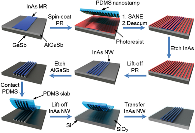
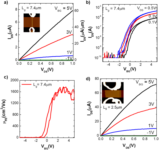
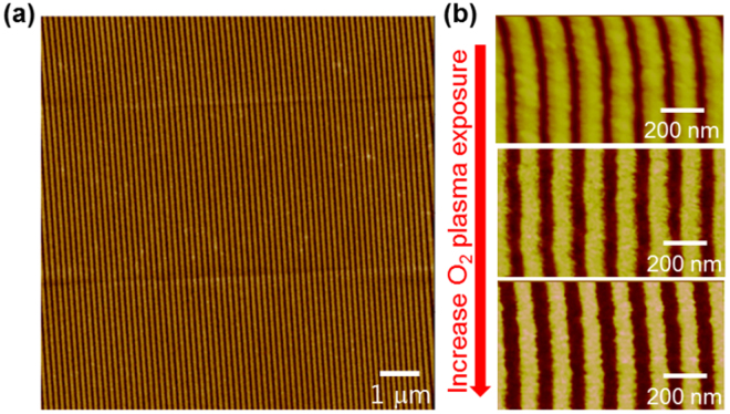
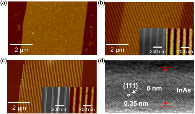
The epitaxial layer transfer process was previously introduced to integrate high-quality and ultrathin III-V compound semiconductor layers on any substrate. However, this technique has limitation for fabrication of sub-micron nanoribbons due to the diffraction limit of photolithography. In order to overcome this limitation and scale down its width to sub-50 nm, we need either a costly short wavelength lithography system or a non-optical patterning method. In this work, high-quality III-V compound semiconductor nanowires were fabricated and integrated onto a Si/SiO substrate by a soft-lithography top-down approach and an epitaxial layer transfer process, using MBE-grown ultrathin InAs as a source wafer. The width of the InAs nanowires was controlled using solvent-assisted nanoscale embossing (SANE), descumming, and etching processes. By optimizing these processes, NWs with a width less than 50 nm were readily obtained. The InAs NWFETs prepared by our method demonstrate peak electron mobility of ~1600 cm/Vs, indicating negligible material degradation during the SANE process.

摘要

外延层转移工艺此前已被引入,用于在任何衬底上集成高质量超薄的III-V族化合物半导体层。然而,由于光刻的衍射极限,该技术在制造亚微米纳米带时存在局限性。为了克服这一局限性并将其宽度缩小至50纳米以下,我们要么需要昂贵的短波长光刻系统,要么需要非光学图案化方法。在这项工作中,通过软光刻自上而下的方法和外延层转移工艺,使用分子束外延(MBE)生长的超薄砷化铟作为源晶片,制造了高质量的III-V族化合物半导体纳米线并将其集成到硅/二氧化硅衬底上。通过溶剂辅助纳米压印(SANE)、去胶和蚀刻工艺控制砷化铟纳米线的宽度。通过优化这些工艺,很容易获得宽度小于50纳米的纳米线。我们的方法制备的砷化铟纳米线场效应晶体管(InAs NWFETs)的峰值电子迁移率约为1600厘米/伏秒,表明在SANE工艺过程中材料降解可忽略不计。

https://cdn.ncbi.nlm.nih.gov/pmc/blobs/5e96/5816620/52ad391eaf00/41598_2018_21420_Fig4_HTML.jpg
https://cdn.ncbi.nlm.nih.gov/pmc/blobs/5e96/5816620/5d6e459724a0/41598_2018_21420_Fig1_HTML.jpg
https://cdn.ncbi.nlm.nih.gov/pmc/blobs/5e96/5816620/b357902e8450/41598_2018_21420_Fig2_HTML.jpg
https://cdn.ncbi.nlm.nih.gov/pmc/blobs/5e96/5816620/57c798cc786d/41598_2018_21420_Fig3_HTML.jpg
https://cdn.ncbi.nlm.nih.gov/pmc/blobs/5e96/5816620/52ad391eaf00/41598_2018_21420_Fig4_HTML.jpg

相似文献

1
A soft lithographic approach to fabricate InAs nanowire field-effect transistors.一种用于制造砷化铟纳米线场效应晶体管的软光刻方法。
Sci Rep. 2018 Feb 16;8(1):3204. doi: 10.1038/s41598-018-21420-y.
2
Uniform and position-controlled InAs nanowires on 2" Si substrates for transistor applications.用于晶体管应用的 2" Si 衬底上具有均匀和位置可控的 InAs 纳米线。
Nanotechnology. 2012 Jan 13;23(1):015302. doi: 10.1088/0957-4484/23/1/015302. Epub 2011 Dec 8.
3
Ultrathin compound semiconductor on insulator layers for high-performance nanoscale transistors.用于高性能纳米尺度晶体管的超薄复合半导体绝缘体层。
Nature. 2010 Nov 11;468(7321):286-9. doi: 10.1038/nature09541.
4
Short-wavelength infrared photodetector on Si employing strain-induced growth of very tall InAs nanowire arrays.基于硅的短波长红外光电探测器,采用应变诱导生长的非常高的砷化铟纳米线阵列。
Sci Rep. 2015 Jun 2;5:10764. doi: 10.1038/srep10764.
5
Effect of ribbon width on electrical transport properties of graphene nanoribbons.带材宽度对石墨烯纳米带电输运性质的影响。
Nano Converg. 2018;5(1):7. doi: 10.1186/s40580-018-0139-0. Epub 2018 Mar 15.
6
Sub-100 nm Si nanowire and nano-sheet array formation by MacEtch using a non-lithographic InAs nanowire mask.使用非光刻的 InAs 纳米线掩模,通过 MacEtch 形成亚 100nm 的 Si 纳米线和纳米片阵列。
Nanotechnology. 2012 Aug 3;23(30):305305. doi: 10.1088/0957-4484/23/30/305305. Epub 2012 Jul 11.
7
High electron mobility InAs nanowire field-effect transistors.高电子迁移率铟砷纳米线场效应晶体管。
Small. 2007 Feb;3(2):326-32. doi: 10.1002/smll.200600379.
8
Nanoscale opening fabrication on Si (111) surface from SiO2 barrier for vertical growth of III-V nanowire arrays.通过SiO₂阻挡层在Si(111)表面制备纳米级开口以实现III-V族纳米线阵列的垂直生长。
Nanotechnology. 2015 Jul 3;26(26):265302. doi: 10.1088/0957-4484/26/26/265302. Epub 2015 Jun 11.
9
Wafer-Scale Epitaxial Growth of an Atomically Thin Single-Crystal Insulator as a Substrate of Two-Dimensional Material Field-Effect Transistors.作为二维材料场效应晶体管衬底的原子级薄单晶绝缘体的晶圆级外延生长。
Nano Lett. 2023 Apr 12;23(7):3054-3061. doi: 10.1021/acs.nanolett.3c00546. Epub 2023 Mar 17.
10
Dimension Engineering of High-Quality InAs Nanostructures on a Wafer Scale.高质量 InAs 纳米结构的晶圆级尺寸工程。
Nano Lett. 2019 Mar 13;19(3):1632-1642. doi: 10.1021/acs.nanolett.8b04561. Epub 2019 Feb 27.

引用本文的文献

1
Engineering multifunctional surface topography to regulate multiple biological responses.设计多功能表面形貌以调控多种生物学反应。
Biomaterials. 2025 Aug;319:123136. doi: 10.1016/j.biomaterials.2025.123136. Epub 2025 Jan 28.
2
Inverse design of perimeter-controlled InAs-assisted metasurface for two-dimensional dynamic beam steering.用于二维动态波束转向的周长控制InAs辅助超表面的逆向设计。
Nanophotonics. 2022 Sep 2;11(20):4515-4530. doi: 10.1515/nanoph-2022-0376. eCollection 2022 Sep.
3
Template-Assisted Iron Nanowire Formation at Different Electrolyte Temperatures.

本文引用的文献

1
Thermal probe maskless lithography for 27.5 nm half-pitch Si technology.用于 27.5nm 半节距硅技术的热探针无掩模光刻。
Nano Lett. 2013 Sep 11;13(9):4485-91. doi: 10.1021/nl4024066. Epub 2013 Aug 23.
2
Ballistic InAs nanowire transistors.弹道 InAs 纳米线晶体管。
Nano Lett. 2013 Feb 13;13(2):555-8. doi: 10.1021/nl3040674. Epub 2013 Jan 3.
3
Carbon nanotube electronics--moving forward.碳纳米管电子学——向前迈进。
不同电解液温度下模板辅助铁纳米线的形成
Materials (Basel). 2021 Jul 22;14(15):4080. doi: 10.3390/ma14154080.
4
Narrower Nanoribbon Biosensors Fabricated by Chemical Lift-off Lithography Show Higher Sensitivity.化学剥离光刻法制备的更窄纳米带生物传感器具有更高的灵敏度。
ACS Nano. 2021 Jan 26;15(1):904-915. doi: 10.1021/acsnano.0c07503. Epub 2020 Dec 18.
Chem Soc Rev. 2013 Apr 7;42(7):2592-609. doi: 10.1039/c2cs35325c.
4
High-mobility and low-power thin-film transistors based on multilayer MoS2 crystals.基于多层 MoS2 晶体的高迁移率和低功耗薄膜晶体管。
Nat Commun. 2012;3:1011. doi: 10.1038/ncomms2018.
5
Self-aligned, extremely high frequency III-V metal-oxide-semiconductor field-effect transistors on rigid and flexible substrates.在刚性和柔性衬底上实现自对准的超高频率 III-V 金属氧化物半导体场效应晶体管。
Nano Lett. 2012 Aug 8;12(8):4140-5. doi: 10.1021/nl301699k. Epub 2012 Jul 3.
6
High-performance single layered WSe₂ p-FETs with chemically doped contacts.具有化学掺杂接触的高性能单层 WSe₂ p-FET。
Nano Lett. 2012 Jul 11;12(7):3788-92. doi: 10.1021/nl301702r. Epub 2012 Jun 19.
7
III-V complementary metal-oxide-semiconductor electronics on silicon substrates.硅衬底上的 III-V 族互补金属氧化物半导体电子学。
Nano Lett. 2012 Jul 11;12(7):3592-5. doi: 10.1021/nl301254z. Epub 2012 Jun 19.
8
Quantifying surface roughness effects on phonon transport in silicon nanowires.量化硅纳米线中表面粗糙度对声子输运的影响。
Nano Lett. 2012 May 9;12(5):2475-82. doi: 10.1021/nl3005868. Epub 2012 Apr 23.
9
Nanometre-scale electronics with III-V compound semiconductors.III-V 族化合物半导体的纳米电子学。
Nature. 2011 Nov 16;479(7373):317-23. doi: 10.1038/nature10677.
10
Multigate transistors as the future of classical metal-oxide-semiconductor field-effect transistors.多栅晶体管——作为经典金属氧化物半导体场效应晶体管的未来。
Nature. 2011 Nov 16;479(7373):310-6. doi: 10.1038/nature10676.