• 文献检索
  • 文档翻译
  • 深度研究
  • 学术资讯
  • Suppr Zotero 插件Zotero 插件
  • 邀请有礼
  • 套餐&价格
  • 历史记录
应用&插件
Suppr Zotero 插件Zotero 插件浏览器插件Mac 客户端Windows 客户端微信小程序
定价
高级版会员购买积分包购买API积分包
服务
文献检索文档翻译深度研究API 文档MCP 服务
关于我们
关于 Suppr公司介绍联系我们用户协议隐私条款
关注我们

Suppr 超能文献

核心技术专利:CN118964589B侵权必究
粤ICP备2023148730 号-1Suppr @ 2026

文献检索

告别复杂PubMed语法,用中文像聊天一样搜索,搜遍4000万医学文献。AI智能推荐,让科研检索更轻松。

立即免费搜索

文件翻译

保留排版,准确专业,支持PDF/Word/PPT等文件格式,支持 12+语言互译。

免费翻译文档

深度研究

AI帮你快速写综述,25分钟生成高质量综述,智能提取关键信息,辅助科研写作。

立即免费体验

极高增益源极栅控晶体管。

Extremely high-gain source-gated transistors.

作者信息

Zhang Jiawei, Wilson Joshua, Auton Gregory, Wang Yiming, Xu Mingsheng, Xin Qian, Song Aimin

机构信息

School of Electrical and Electronic Engineering, University of Manchester, Manchester M13 9PL, United Kingdom.

National Graphene Institute, University of Manchester, Manchester M13 9PL, United Kingdom.

出版信息

Proc Natl Acad Sci U S A. 2019 Mar 12;116(11):4843-4848. doi: 10.1073/pnas.1820756116. Epub 2019 Feb 25.

DOI:10.1073/pnas.1820756116
PMID:30804190
原文链接:https://pmc.ncbi.nlm.nih.gov/articles/PMC6421470/
Abstract

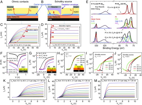
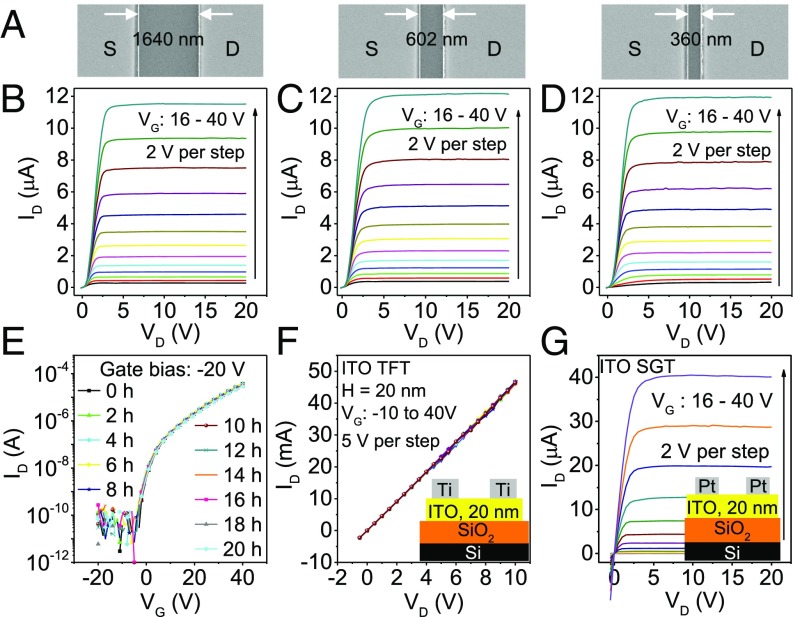
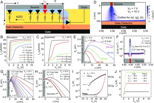
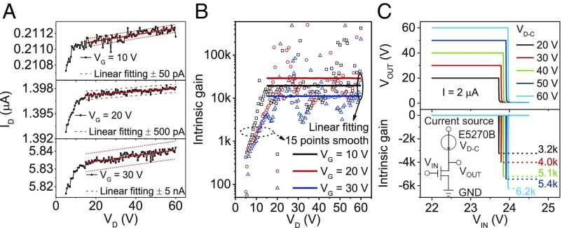
Despite being a fundamental electronic component for over 70 years, it is still possible to develop different transistor designs, including the addition of a diode-like Schottky source electrode to thin-film transistors. The discovery of a dependence of the source barrier height on the semiconductor thickness and derivation of an analytical theory allow us to propose a design rule to achieve extremely high voltage gain, one of the most important figures of merit for a transistor. Using an oxide semiconductor, an intrinsic gain of 29,000 was obtained, which is orders of magnitude higher than a conventional Si transistor. These same devices demonstrate almost total immunity to negative bias illumination temperature stress, the foremost bottleneck to using oxide semiconductors in major applications, such as display drivers. Furthermore, devices fabricated with channel lengths down to 360 nm display no obvious short-channel effects, another critical factor for high-density integrated circuits and display applications. Finally, although the channel material of conventional transistors must be a semiconductor, by demonstrating a high-performance transistor with a semimetal-like indium tin oxide channel, the range and versatility of materials have been significantly broadened.

摘要

尽管晶体管作为一种基本电子元件已有70多年历史,但仍有可能开发出不同的晶体管设计,包括在薄膜晶体管中添加类似二极管的肖特基源电极。源极势垒高度与半导体厚度的相关性的发现以及解析理论的推导,使我们能够提出一种设计规则,以实现极高的电压增益,这是晶体管最重要的品质因数之一。使用氧化物半导体,获得了29000的本征增益,比传统硅晶体管高出几个数量级。这些器件几乎完全不受负偏置光照温度应力的影响,而负偏置光照温度应力是在诸如显示驱动器等主要应用中使用氧化物半导体的首要瓶颈。此外,沟道长度低至360 nm的器件没有明显的短沟道效应,这是高密度集成电路和显示应用的另一个关键因素。最后,尽管传统晶体管的沟道材料必须是半导体,但通过展示具有类半金属铟锡氧化物沟道的高性能晶体管,材料的范围和通用性得到了显著拓宽。

https://cdn.ncbi.nlm.nih.gov/pmc/blobs/e3d5/6421470/4c25c53c33e0/pnas.1820756116fig04.jpg
https://cdn.ncbi.nlm.nih.gov/pmc/blobs/e3d5/6421470/65007281cad3/pnas.1820756116fig01.jpg
https://cdn.ncbi.nlm.nih.gov/pmc/blobs/e3d5/6421470/0c32b41fe5d4/pnas.1820756116fig02.jpg
https://cdn.ncbi.nlm.nih.gov/pmc/blobs/e3d5/6421470/6fff6a77ea0c/pnas.1820756116fig03.jpg
https://cdn.ncbi.nlm.nih.gov/pmc/blobs/e3d5/6421470/4c25c53c33e0/pnas.1820756116fig04.jpg

相似文献

1
Extremely high-gain source-gated transistors.极高增益源极栅控晶体管。
Proc Natl Acad Sci U S A. 2019 Mar 12;116(11):4843-4848. doi: 10.1073/pnas.1820756116. Epub 2019 Feb 25.
2
Novel Tunnel-Contact-Controlled IGZO Thin-Film Transistors with High Tolerance to Geometrical Variability.具有高几何变化耐受性的新型隧道接触控制铟镓锌氧化物薄膜晶体管
Adv Mater. 2019 Sep;31(36):e1902551. doi: 10.1002/adma.201902551. Epub 2019 Jul 16.
3
Subthreshold Schottky-barrier thin-film transistors with ultralow power and high intrinsic gain.亚阈值肖特基势垒薄膜晶体管具有超低功耗和高本征增益。
Science. 2016 Oct 21;354(6310):302-304. doi: 10.1126/science.aah5035.
4
Indium-Tin-Oxide Transistors with One Nanometer Thick Channel and Ferroelectric Gating.具有一纳米厚沟道和铁电栅极的铟锡氧化物晶体管。
ACS Nano. 2020 Sep 22;14(9):11542-11547. doi: 10.1021/acsnano.0c03978. Epub 2020 Aug 26.
5
High-Performance Organic Source-Gated Transistors Enabled by the Indium-Tin Oxide-Diketopyrrolopyrrole Polymer Interface.由氧化铟锡-二酮吡咯并吡咯聚合物界面实现的高性能有机源极栅控晶体管。
ACS Appl Mater Interfaces. 2023 Mar 1;15(8):10918-10925. doi: 10.1021/acsami.2c22350. Epub 2023 Feb 17.
6
Schottky barrier thin film transistors using solution-processed n-ZnO.采用溶液法制备的 n-ZnO 的肖特基势垒薄膜晶体管。
ACS Appl Mater Interfaces. 2012 Mar;4(3):1423-8. doi: 10.1021/am201656h. Epub 2012 Mar 12.
7
High Performance Indium-Tin-Oxide Schottky Diodes for Terahertz Band Operation.用于太赫兹波段操作的高性能铟锡氧化物肖特基二极管。
Nano Lett. 2024 Jul 3;24(26):7919-7926. doi: 10.1021/acs.nanolett.4c01172. Epub 2024 Jun 5.
8
Impact of transient currents caused by alternating drain stress in oxide semiconductors.氧化物半导体中交流漏极应力引起的瞬态电流的影响。
Sci Rep. 2017 Aug 29;7(1):9782. doi: 10.1038/s41598-017-10285-2.
9
Multiple Schottky Barrier-Limited Field-Effect Transistors on a Single Silicon Nanowire with an Intrinsic Doping Gradient.单个硅纳米线内固有掺杂梯度上的多个肖特基势垒限制场效应晶体管。
ACS Appl Mater Interfaces. 2017 Apr 5;9(13):12046-12053. doi: 10.1021/acsami.7b00144. Epub 2017 Mar 23.
10
Analytical modeling of trilayer graphene nanoribbon Schottky-barrier FET for high-speed switching applications.三层石墨烯纳米带肖特基势垒 FET 的高速开关应用分析建模。
Nanoscale Res Lett. 2013 Jan 30;8(1):55. doi: 10.1186/1556-276X-8-55.

引用本文的文献

1
The Origin of Low Contact Resistance in Monolayer Organic Field-Effect Transistors with van der Waals Electrodes.具有范德华电极的单层有机场效应晶体管中低接触电阻的起源
Small Sci. 2022 Mar 7;2(6):2100115. doi: 10.1002/smsc.202100115. eCollection 2022 Jun.
2
Super-saturated complementary carbon nanotube transistors with intrinsic gain singularities.具有本征增益奇点的超饱和互补碳纳米管晶体管。
Nat Commun. 2025 Apr 10;16(1):3390. doi: 10.1038/s41467-025-58399-w.
3
Ultrahigh-gain organic transistors based on van der Waals metal-barrier interlayer-semiconductor junction.

本文引用的文献

1
Interfacial Chemistry-Induced Modulation of Schottky Barrier Heights: In Situ Measurements of the Pt-Amorphous Indium Gallium Zinc Oxide Interface Using X-ray Photoelectron Spectroscopy.界面化学诱导肖特基势垒高度调制:使用 X 射线光电子能谱原位测量 Pt-非晶态铟镓锌氧化物界面。
ACS Appl Mater Interfaces. 2018 Jan 31;10(4):4333-4340. doi: 10.1021/acsami.7b18674. Epub 2018 Jan 18.
2
Subthreshold Schottky-barrier thin-film transistors with ultralow power and high intrinsic gain.亚阈值肖特基势垒薄膜晶体管具有超低功耗和高本征增益。
Science. 2016 Oct 21;354(6310):302-304. doi: 10.1126/science.aah5035.
3
Single-crystalline ZnO sheet Source-Gated Transistors.
基于范德华金属势垒层间半导体结的超高增益有机晶体管。
Sci Adv. 2023 Dec 8;9(49):eadj4656. doi: 10.1126/sciadv.adj4656. Epub 2023 Dec 6.
4
High-performance and low-power source-gated transistors enabled by a solution-processed metal oxide homojunction.通过溶液处理的金属氧化物同质结实现的高性能、低功耗源栅晶体管。
Proc Natl Acad Sci U S A. 2023 Jan 17;120(3):e2216672120. doi: 10.1073/pnas.2216672120. Epub 2023 Jan 11.
5
New Opportunities for High-Performance Source-Gated Transistors Using Unconventional Materials.使用非常规材料的高性能源极栅控晶体管的新机遇。
Adv Sci (Weinh). 2021 Oct;8(20):e2101473. doi: 10.1002/advs.202101473. Epub 2021 Aug 27.
6
Experimental and theoretical evidence for hydrogen doping in polymer solution-processed indium gallium oxide.聚合物溶液处理的氧化铟镓中氢掺杂的实验与理论证据。
Proc Natl Acad Sci U S A. 2020 Aug 4;117(31):18231-18239. doi: 10.1073/pnas.2007897117. Epub 2020 Jul 23.
单晶氧化锌片源极栅控晶体管。
Sci Rep. 2016 Jan 13;6:19232. doi: 10.1038/srep19232.
4
Flexible indium-gallium-zinc-oxide Schottky diode operating beyond 2.45 GHz.工作频率超过 2.45GHz 的柔性铟镓锌氧化物肖特基二极管。
Nat Commun. 2015 Jul 3;6:7561. doi: 10.1038/ncomms8561.
5
Source-gated transistors for order-of-magnitude performance improvements in thin-film digital circuits.用于大幅提升薄膜数字电路性能的源极门控晶体管。
Sci Rep. 2014 Mar 6;4:4295. doi: 10.1038/srep04295.
6
Oxide semiconductor thin-film transistors: a review of recent advances.氧化物半导体薄膜晶体管:研究进展综述。
Adv Mater. 2012 Jun 12;24(22):2945-86. doi: 10.1002/adma.201103228. Epub 2012 May 10.
7
Room-temperature fabrication of transparent flexible thin-film transistors using amorphous oxide semiconductors.使用非晶氧化物半导体在室温下制备透明柔性薄膜晶体管。
Nature. 2004 Nov 25;432(7016):488-92. doi: 10.1038/nature03090.
8
Thin-film transistor fabricated in single-crystalline transparent oxide semiconductor.采用单晶透明氧化物半导体制备的薄膜晶体管。
Science. 2003 May 23;300(5623):1269-72. doi: 10.1126/science.1083212.