Li Zhen-Ze, Wang Lei, Fan Hua, Yu Yan-Hao, Sun Hong-Bo, Juodkazis Saulius, Chen Qi-Dai
1State Key Laboratory of Integrated Optoelectronics, College of Electronic Science and Engineering, Jilin University, Changchun, 130012 China.
2State Key Laboratory of Precision Measurement Technology and Instruments, Department of Precision Instrument, Tsinghua University, Beijing, 100084 China.
Light Sci Appl. 2020 Mar 16;9:41. doi: 10.1038/s41377-020-0275-2. eCollection 2020.
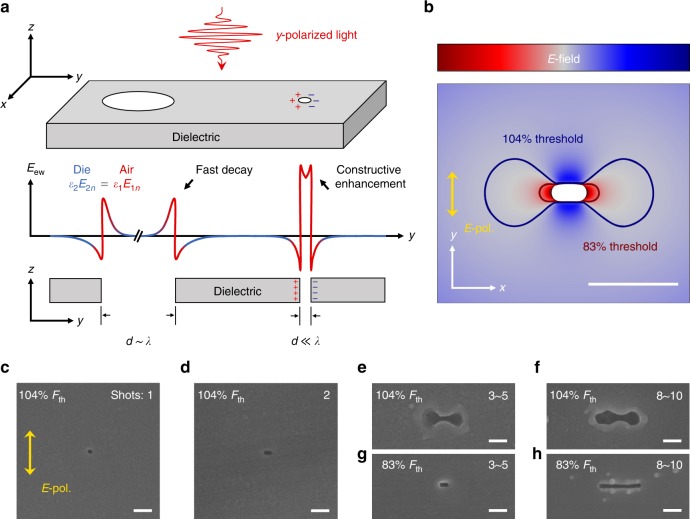
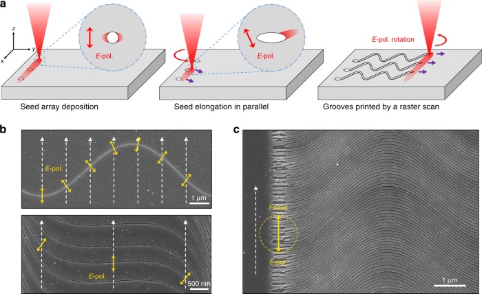
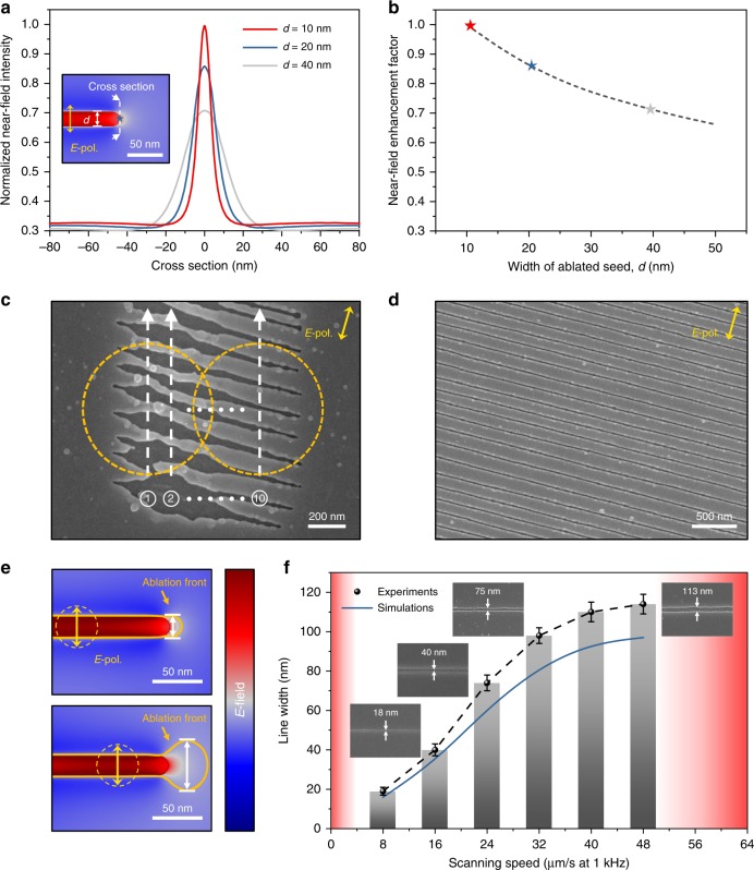
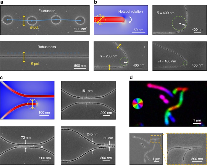
Nanoscale surface texturing, drilling, cutting, and spatial sculpturing, which are essential for applications, including thin-film solar cells, photonic chips, antireflection, wettability, and friction drag reduction, require not only high accuracy in material processing, but also the capability of manufacturing in an atmospheric environment. Widely used focused ion beam (FIB) technology offers nanoscale precision, but is limited by the vacuum-working conditions; therefore, it is not applicable to industrial-scale samples such as ship hulls or biomaterials, e.g., cells and tissues. Here, we report an optical far-field-induced near-field breakdown (O-FIB) approach as an optical version of the conventional FIB technique, which allows direct nanowriting in air. The writing is initiated from nanoholes created by femtosecond-laser-induced multiphoton absorption, and its cutting "knife edge" is sharpened by the far-field-regulated enhancement of the optical near field. A spatial resolution of less than 20 nm (/40, with being the light wavelength) is readily achieved. O-FIB is empowered by the utilization of simple polarization control of the incident light to steer the nanogroove writing along the designed pattern. The universality of near-field enhancement and localization makes O-FIB applicable to various materials, and enables a large-area printing mode that is superior to conventional FIB processing.
纳米级表面纹理化、钻孔、切割和空间雕刻对于包括薄膜太阳能电池、光子芯片、抗反射、润湿性和减阻等应用至关重要,这些不仅需要材料加工的高精度,还需要在大气环境中进行制造的能力。广泛使用的聚焦离子束(FIB)技术提供了纳米级精度,但受限于真空工作条件;因此,它不适用于诸如船体或生物材料(如细胞和组织)等工业规模的样品。在此,我们报告一种光学远场诱导近场击穿(O-FIB)方法,作为传统FIB技术的光学版本,它允许在空气中直接进行纳米写入。写入从飞秒激光诱导多光子吸收产生的纳米孔开始,其切割“刀刃”通过光学近场的远场调节增强而变尖锐。易于实现小于20 nm(/40,其中 为光波长)的空间分辨率。通过利用入射光的简单偏振控制来沿着设计图案引导纳米槽写入,O-FIB得以实现。近场增强和局域化的普遍性使O-FIB适用于各种材料,并实现了优于传统FIB加工的大面积打印模式。