Ben Moussa Nizar, Lajnef Mohamed, Jebari Nessrine, Villebasse Cedric, Bayle Fabien, Chaste Julien, Madouri Ali, Chtourou Radouane, Herth Etienne
Centre de Nanosciences et de Nanotechnologies, CNRS UMR 9001, Univ. Paris-Sud, Université Paris-Saclay Palaiseau 91120 France
Laboratory of Nanomaterials and Systems for Renewable Energies (LaNSER), Research and Technologies Centre of Energy, Faculty of Sciences of Tunis, University of Tunis El Manar Technopark Borj Cedria BP 095 Hammam Lif Tunisia.
RSC Adv. 2021 Jun 29;11(37):22723-22733. doi: 10.1039/d1ra02241e. eCollection 2021 Jun 25.
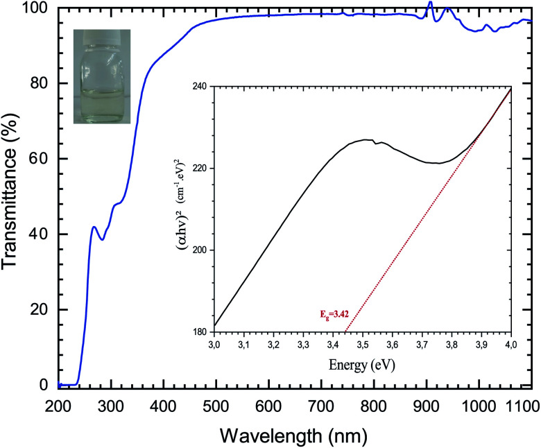
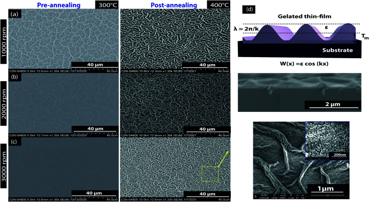
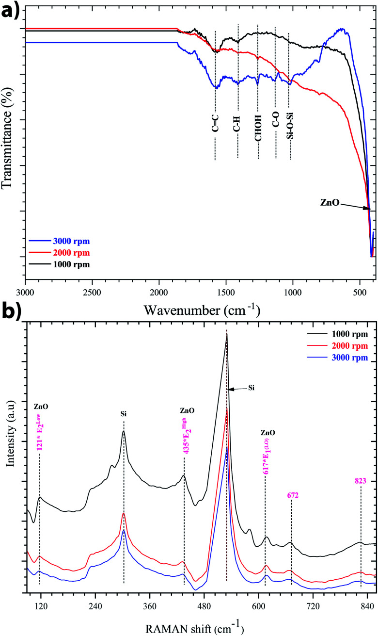
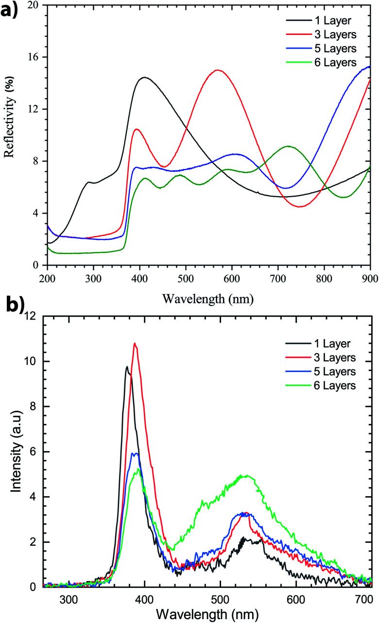
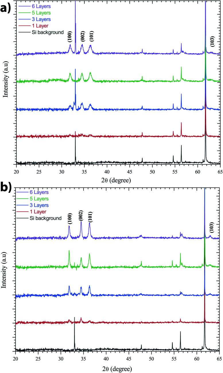
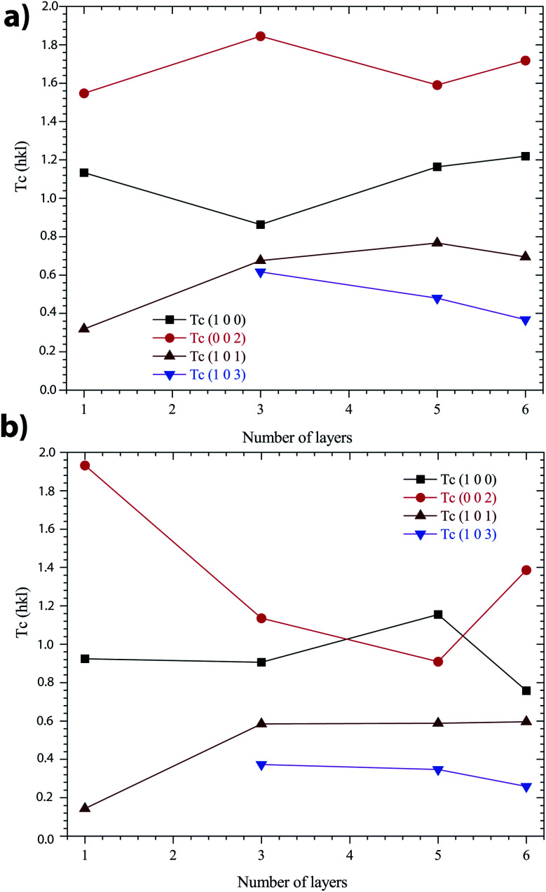
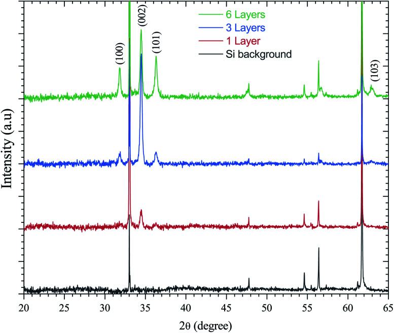
Zinc oxide (ZnO) is a II-VI group semiconductor with a wide direct bandgap and is an important material for various fields of industry and high-technological applications. The effects of thickness, annealing process in N and air, optical properties, and morphology of ZnO thin-films are studied. A low-cost sol-gel spin-coating technique is used in this study for the simple synthesis of eco-friendly ZnO multilayer films deposited on (100)-oriented silicon substrates ranging from 150 to 600 nm by adjusting the spin coating rate. The ZnO sol-gel thin-films using precursor solutions of molarity 0.75 M exhibit an average optical transparency above 98%, with an optical band gap energy of 3.42 eV. The -axis (002) orientation of the ZnO thin-films annealed at 400 °C were mainly influenced by the thickness of the multilayer, which is of interest for piezoelectric applications. These results demonstrate that a low-temperature method can be used to produce an eco-friendly, cost-effective ZnO sol-gel that is compatible with a complementary metal-oxide-semiconductor (CMOS) and integrated-circuits (IC).
氧化锌(ZnO)是一种具有宽直接带隙的II-VI族半导体,是工业和高科技应用各个领域的重要材料。研究了ZnO薄膜的厚度、在氮气和空气中的退火工艺、光学性质以及形貌。本研究采用低成本的溶胶-凝胶旋涂技术,通过调整旋涂速率,在(100)取向的硅衬底上简单合成了厚度在150至600纳米之间的环保型ZnO多层膜。使用摩尔浓度为0.75 M的前驱体溶液制备的ZnO溶胶-凝胶薄膜平均光学透明度高于98%,光学带隙能量为3.42 eV。在400°C退火的ZnO薄膜的c轴(002)取向主要受多层膜厚度的影响,这在压电应用中具有重要意义。这些结果表明,低温方法可用于制备与互补金属氧化物半导体(CMOS)和集成电路(IC)兼容的环保、经济高效的ZnO溶胶-凝胶。