Nassiopoulou Androula Galiouna, Gianneta Violetta, Katsogridakis Charalambos
Institute of Microelectronics (IMEL), National Center for Scientific Research (NCSR) Demokritos, Terma Patriarhou Gregoriou, Aghia Paraskevi, Athens, 15310, Greece.
Nanoscale Res Lett. 2011 Nov 16;6(1):597. doi: 10.1186/1556-276X-6-597.
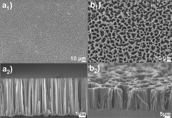
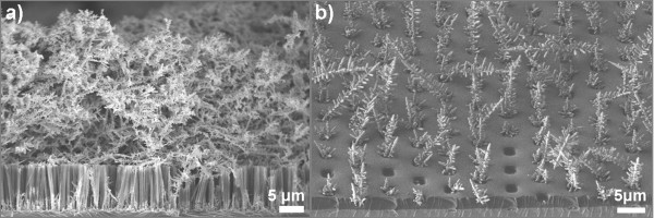
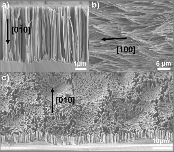
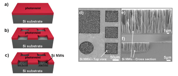
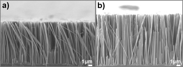
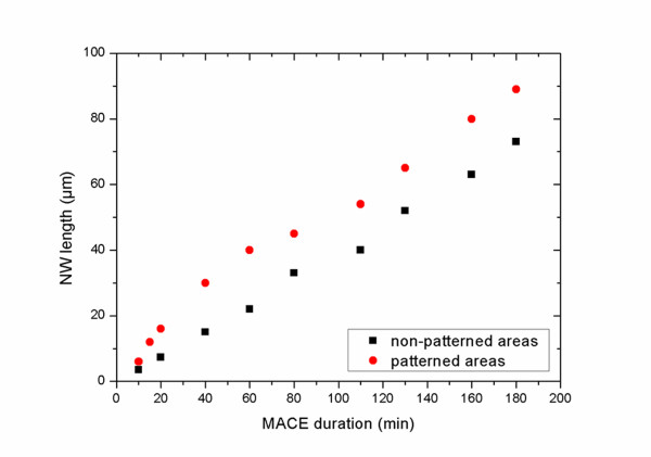
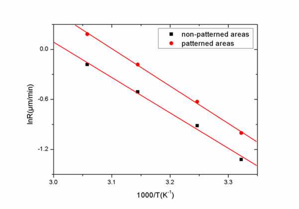
In this paper, we investigate the formation kinetics of Si nanowires [SiNWs] on lithographically defined areas using a single-step metal-assisted chemical etching process in an aqueous HF/AgNO3 solution. We show that the etch rate of Si, and consequently, the SiNW length, is much higher on the lithographically defined areas compared with that on the non-patterned areas. A comparative study of the etch rate in the two cases under the same experimental conditions showed that this effect is much more pronounced at the beginning of the etching process. Moreover, it was found that in both cases, the nanowire formation rate is linear with temperature in the range from 20°C to 50°C, with almost the same activation energy, as obtained from an Arrhenius plot (0.37 eV in the case of non-patterned areas, while 0.38 eV in the case of lithographically patterned areas). The higher etch rate on lithographically defined areas is mainly attributed to Si surface modification during the photolithographic process.PACS: 68; 68.65-k.
在本文中,我们使用一步金属辅助化学蚀刻工艺,在水性HF/AgNO₃溶液中,研究光刻定义区域上硅纳米线[SiNWs]的形成动力学。我们表明,与未图案化区域相比,光刻定义区域上硅的蚀刻速率以及相应的硅纳米线长度要高得多。在相同实验条件下对两种情况的蚀刻速率进行的比较研究表明,这种效应在蚀刻过程开始时更为明显。此外,发现在两种情况下,纳米线形成速率在20°C至50°C范围内与温度呈线性关系,从阿仑尼乌斯图获得的活化能几乎相同(未图案化区域为0.37 eV,光刻图案化区域为0.38 eV)。光刻定义区域上较高的蚀刻速率主要归因于光刻过程中硅表面的改性。物理和化学主题分类号:68;68.65 - k。