Department of Physics, Interdepartmental Centre NIS, University of Torino, via Giuria 1, 10125, Torino, Italy.
Department of Chemistry, Interdepartmental Centre NIS, University of Torino, via Giuria 7, 10125, Torino, Italy.
Sci Rep. 2017 Aug 22;7(1):9066. doi: 10.1038/s41598-017-09443-3.
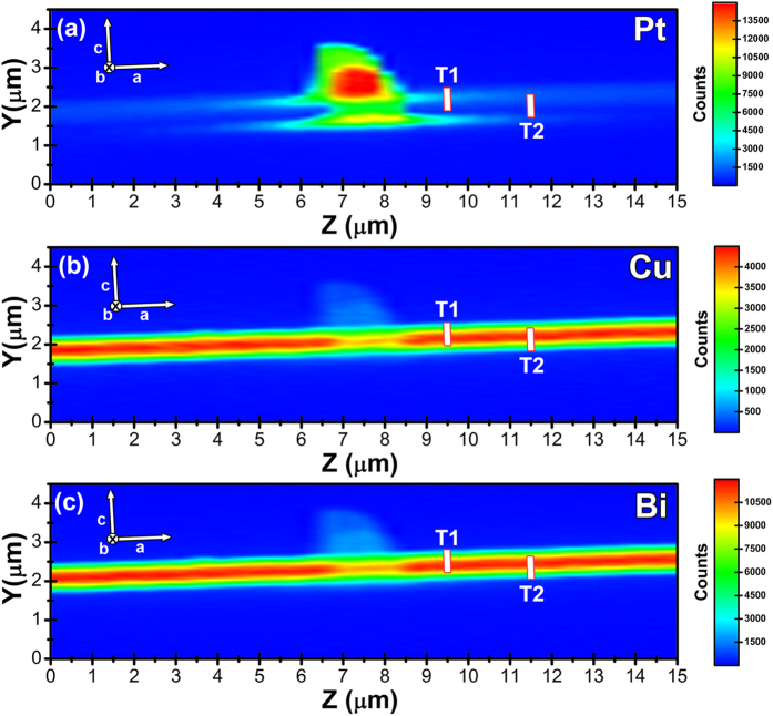
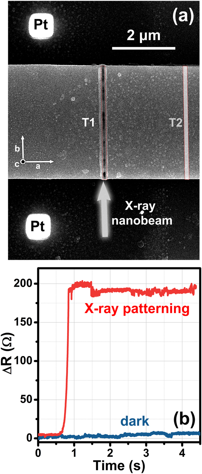
X-ray nanofabrication has so far been usually limited to mask methods involving photoresist impression and subsequent etching. Herein we show that an innovative maskless X-ray nanopatterning approach allows writing electrical devices with nanometer feature size. In particular we fabricated a Josephson device on a BiSrCaCuO (Bi-2212) superconducting oxide micro-crystal by drawing two single lines of only 50 nm in width using a 17.4 keV synchrotron nano-beam. A precise control of the fabrication process was achieved by monitoring in situ the variations of the device electrical resistance during X-ray irradiation, thus finely tuning the irradiation time to drive the material into a non-superconducting state only in the irradiated regions, without significantly perturbing the crystal structure. Time-dependent finite element model simulations show that a possible microscopic origin of this effect can be related to the instantaneous temperature increase induced by the intense synchrotron picosecond X-ray pulses. These results prove that a conceptually new patterning method for oxide electrical devices, based on the local change of electrical properties, is actually possible with potential advantages in terms of heat dissipation, chemical contamination, miniaturization and high aspect ratio of the devices.
X 射线纳米光刻技术迄今为止通常限于涉及光刻胶压印和后续刻蚀的掩模方法。本文展示了一种创新的无掩模 X 射线纳米光刻方法,可用于写入具有纳米特征尺寸的电子器件。具体来说,我们通过使用 17.4keV 同步加速器纳米束在 BiSrCaCuO(Bi-2212)超导氧化物微晶体上绘制仅 50nm 宽的两条单线条,制造了一个约瑟夫森器件。通过原位监测 X 射线照射过程中器件电阻的变化,精确控制了制造过程,从而精细地调整照射时间,仅在照射区域将材料驱动到非超导状态,而不会显著干扰晶体结构。基于时间的有限元模型模拟表明,这种效应的一种可能的微观起源可以与强同步加速器皮秒 X 射线脉冲引起的瞬时温度升高有关。这些结果证明,基于电特性局部变化的氧化物电子器件的一种全新的图案化方法实际上是可行的,这种方法在散热、化学污染、小型化和器件高纵横比方面具有潜在优势。