Shang Chen, Feng Kaiyin, Hughes Eamonn T, Clark Andrew, Debnath Mukul, Koscica Rosalyn, Leake Gerald, Herman Joshua, Harame David, Ludewig Peter, Wan Yating, Bowers John E
Materials Department, University of California Santa Barbara, Santa Barbara, CA, 93106, USA.
Department of Electrical and Computer Engineering, University of California Santa Barbara, Santa Barbara, CA, 93106, USA.
Light Sci Appl. 2022 Oct 14;11(1):299. doi: 10.1038/s41377-022-00982-7.
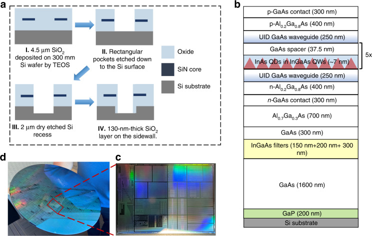
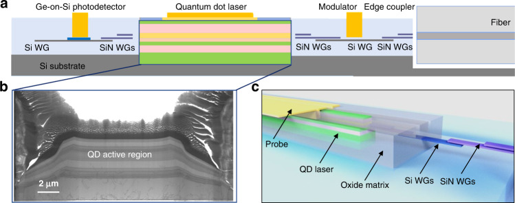
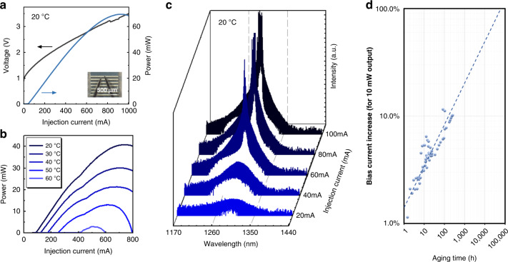
Monolithic integration of quantum dot (QD) gain materials onto Si photonic platforms via direct epitaxial growth is a promising solution for on-chip light sources. Recent developments have demonstrated superior device reliability in blanket hetero-epitaxy of III-V devices on Si at elevated temperatures. Yet, thick, defect management epi designs prevent vertical light coupling from the gain region to the Si-on-Insulator waveguides. Here, we demonstrate the first electrically pumped QD lasers grown by molecular beam epitaxy on a 300 mm patterned (001) Si wafer with a butt-coupled configuration. Unique growth and fabrication challenges imposed by the template architecture have been resolved, contributing to continuous wave lasing to 60 °C and a maximum double-side output power of 126.6 mW at 20 °C with a double-side wall-plug efficiency of 8.6%. The potential for robust on-chip laser operation and efficient low-loss light coupling to Si photonic circuits makes this heteroepitaxial integration platform on Si promising for scalable and low-cost mass production.
通过直接外延生长将量子点(QD)增益材料单片集成到硅光子平台上,是实现片上光源的一种很有前景的解决方案。最近的进展表明,在高温下在硅上进行III-V族器件的毯式异质外延具有卓越的器件可靠性。然而,厚的、用于缺陷管理的外延设计阻碍了从增益区到绝缘体上硅波导的垂直光耦合。在此,我们展示了首个通过分子束外延在具有对接耦合结构的300毫米图案化(001)硅晶圆上生长的电泵浦量子点激光器。模板架构带来的独特生长和制造挑战已得到解决,实现了在60°C下连续波激射,在20°C时最大双侧输出功率为126.6毫瓦,双侧壁插效率为8.6%。这种在硅上进行稳健的片上激光操作以及与硅光子电路进行高效低损耗光耦合的潜力,使得这种硅上异质外延集成平台有望实现可扩展的低成本大规模生产。