• 文献检索
  • 文档翻译
  • 深度研究
  • 学术资讯
  • Suppr Zotero 插件Zotero 插件
  • 邀请有礼
  • 套餐&价格
  • 历史记录
应用&插件
Suppr Zotero 插件Zotero 插件浏览器插件Mac 客户端Windows 客户端微信小程序
定价
高级版会员购买积分包购买API积分包
服务
文献检索文档翻译深度研究API 文档MCP 服务
关于我们
关于 Suppr公司介绍联系我们用户协议隐私条款
关注我们

Suppr 超能文献

核心技术专利:CN118964589B侵权必究
粤ICP备2023148730 号-1Suppr @ 2026

文献检索

告别复杂PubMed语法,用中文像聊天一样搜索,搜遍4000万医学文献。AI智能推荐,让科研检索更轻松。

立即免费搜索

文件翻译

保留排版,准确专业,支持PDF/Word/PPT等文件格式,支持 12+语言互译。

免费翻译文档

深度研究

AI帮你快速写综述,25分钟生成高质量综述,智能提取关键信息,辅助科研写作。

立即免费体验

在绝缘体上硅(SOI)上实现嵌入式III-V族激光器的单片集成。

Monolithic integration of embedded III-V lasers on SOI.

作者信息

Wei Wen-Qi, He An, Yang Bo, Wang Zi-Hao, Huang Jing-Zhi, Han Dong, Ming Ming, Guo Xuhan, Su Yikai, Zhang Jian-Jun, Wang Ting

机构信息

Institute of Physics, Chinese Academy of Sciences, Beijing, China.

Songshan Lake Materials Laboratory, Dongguan, Guangdong, China.

出版信息

Light Sci Appl. 2023 Apr 3;12(1):84. doi: 10.1038/s41377-023-01128-z.

DOI:10.1038/s41377-023-01128-z
PMID:37009809
原文链接:https://pmc.ncbi.nlm.nih.gov/articles/PMC10068801/
Abstract

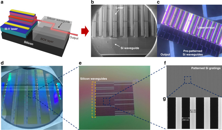
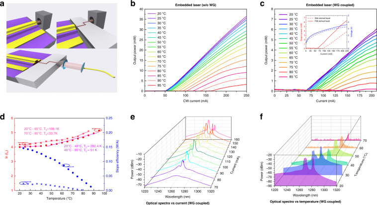
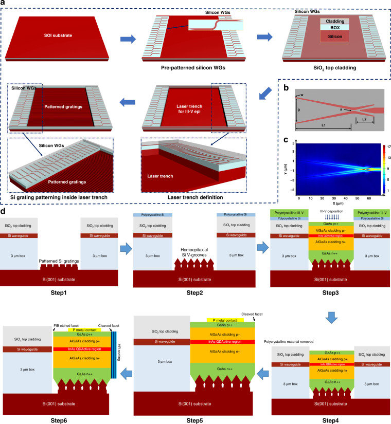
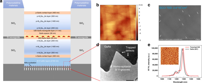
Silicon photonic integration has gained great success in many application fields owing to the excellent optical device properties and complementary metal-oxide semiconductor (CMOS) compatibility. Realizing monolithic integration of III-V lasers and silicon photonic components on single silicon wafer is recognized as a long-standing obstacle for ultra-dense photonic integration, which can provide considerable economical, energy-efficient and foundry-scalable on-chip light sources, that has not been reported yet. Here, we demonstrate embedded InAs/GaAs quantum dot (QD) lasers directly grown on trenched silicon-on-insulator (SOI) substrate, enabling monolithic integration with butt-coupled silicon waveguides. By utilizing the patterned grating structures inside pre-defined SOI trenches and unique epitaxial method via hybrid molecular beam epitaxy (MBE), high-performance embedded InAs QD lasers with monolithically out-coupled silicon waveguide are achieved on such template. By resolving the epitaxy and fabrication challenges in such monolithic integrated architecture, embedded III-V lasers on SOI with continuous-wave lasing up to 85 °C are obtained. The maximum output power of 6.8 mW can be measured from the end tip of the butt-coupled silicon waveguides, with estimated coupling efficiency of approximately -6.7 dB. The results presented here provide a scalable and low-cost epitaxial method for the realization of on-chip light sources directly coupling to the silicon photonic components for future high-density photonic integration.

摘要

由于具有出色的光学器件特性以及与互补金属氧化物半导体(CMOS)的兼容性,硅光子集成在许多应用领域都取得了巨大成功。在单晶硅片上实现III-V族激光器与硅光子组件的单片集成,被认为是超密集光子集成长期以来的一个障碍,而这种集成可以提供经济高效且具有可扩展性的片上光源,但目前尚未见相关报道。在此,我们展示了直接生长在刻蚀绝缘体上硅(SOI)衬底上的嵌入式InAs/GaAs量子点(QD)激光器,实现了与对接耦合硅波导的单片集成。通过利用预定义SOI沟槽内的图案化光栅结构以及混合分子束外延(MBE)的独特外延方法,在这种模板上实现了具有单片外耦合硅波导的高性能嵌入式InAs量子点激光器。通过解决这种单片集成架构中的外延和制造难题,获得了在高达85°C的温度下连续波激射的SOI上的嵌入式III-V族激光器。从对接耦合硅波导的末端可以测量到最大输出功率为6.8 mW,估计耦合效率约为 -6.7 dB。本文给出的结果为实现直接与硅光子组件耦合的片上光源提供了一种可扩展且低成本的外延方法,以用于未来的高密度光子集成。

https://cdn.ncbi.nlm.nih.gov/pmc/blobs/1b77/10068801/3106453d80b0/41377_2023_1128_Fig5_HTML.jpg
https://cdn.ncbi.nlm.nih.gov/pmc/blobs/1b77/10068801/a7105520eae5/41377_2023_1128_Fig1_HTML.jpg
https://cdn.ncbi.nlm.nih.gov/pmc/blobs/1b77/10068801/0532e335fad8/41377_2023_1128_Fig2_HTML.jpg
https://cdn.ncbi.nlm.nih.gov/pmc/blobs/1b77/10068801/9618fd7e0a9f/41377_2023_1128_Fig3_HTML.jpg
https://cdn.ncbi.nlm.nih.gov/pmc/blobs/1b77/10068801/31f57c658305/41377_2023_1128_Fig4_HTML.jpg
https://cdn.ncbi.nlm.nih.gov/pmc/blobs/1b77/10068801/3106453d80b0/41377_2023_1128_Fig5_HTML.jpg

相似文献

1
Monolithic integration of embedded III-V lasers on SOI.在绝缘体上硅(SOI)上实现嵌入式III-V族激光器的单片集成。
Light Sci Appl. 2023 Apr 3;12(1):84. doi: 10.1038/s41377-023-01128-z.
2
InAs/GaAs quantum dot narrow ridge lasers epitaxially grown on SOI substrates for silicon photonic integration.用于硅光子集成的在绝缘体上硅(SOI)衬底上外延生长的砷化铟/砷化镓量子点窄脊激光器。
Opt Express. 2020 Aug 31;28(18):26555-26563. doi: 10.1364/OE.402174.
3
Electrically pumped quantum-dot lasers grown on 300 mm patterned Si photonic wafers.生长在300毫米图案化硅光子晶圆上的电泵浦量子点激光器。
Light Sci Appl. 2022 Oct 14;11(1):299. doi: 10.1038/s41377-022-00982-7.
4
Unlocking the monolithic integration scenario: optical coupling between GaSb diode lasers epitaxially grown on patterned Si substrates and passive SiN waveguides.开启单片集成方案:在图案化硅衬底上外延生长的锑化镓二极管激光器与无源氮化硅波导之间的光耦合。
Light Sci Appl. 2023 Jun 16;12(1):150. doi: 10.1038/s41377-023-01185-4.
5
P-doped 1300  nm InAs/GaAs quantum dot lasers directly grown on an SOI substrate.直接生长在硅基绝缘体(SOI)衬底上的P掺杂1300纳米砷化铟/砷化镓量子点激光器。
Opt Lett. 2021 Nov 1;46(21):5525-5528. doi: 10.1364/OL.437471.
6
1310 nm InAs quantum-dot microdisk lasers on SOI by hybrid epitaxy.基于混合外延的硅基绝缘体上1310纳米砷化铟量子点微盘激光器
Opt Express. 2019 Jul 8;27(14):19348-19358. doi: 10.1364/OE.27.019348.
7
Reduction of GaAs Buffer Thickness and Its Impact on Epitaxially Integrated III-V Quantum Dot Lasers on a Si Substrate.降低砷化镓缓冲层厚度及其对硅衬底上外延集成的III-V族量子点激光器的影响。
ACS Appl Mater Interfaces. 2024 Jun 12;16(23):30209-30217. doi: 10.1021/acsami.4c04597. Epub 2024 Jun 3.
8
Continuous-wave quantum dot photonic crystal lasers grown on on-axis Si (001).在轴向硅(001)上生长的连续波光量子点光子晶体激光器。
Nat Commun. 2020 Feb 20;11(1):977. doi: 10.1038/s41467-020-14736-9.
9
E-Band InAs Quantum Dot Micro-Disk Laser with Metamorphic InGaAs Layers Grown on GaAs/Si (001) Substrate.在GaAs/Si(001)衬底上生长有变质InGaAs层的E波段InAs量子点微盘激光器。
Materials (Basel). 2024 Apr 21;17(8):1916. doi: 10.3390/ma17081916.
10
Phosphorus-free 1.5  µm InAs quantum-dot microdisk lasers on metamorphic InGaAs/SOI platform.基于变质InGaAs/SOI平台的无磷1.5微米砷化铟量子点微盘激光器。
Opt Lett. 2020 Apr 1;45(7):2042-2045. doi: 10.1364/OL.389191.

引用本文的文献

1
Demonstration of Monolithic Integration of InAs Quantum Dot Microdisk Light Emitters and Photodetectors Directly Grown on On-Axis Silicon (001).在轴向上生长于硅(001)上的砷化铟量子点微盘发光器和光电探测器的单片集成演示。
Micromachines (Basel). 2025 Jul 31;16(8):897. doi: 10.3390/mi16080897.
2
Numerical Analysis of a SiN Digital Fourier Transform Spectrometer for a Non-Invasive Skin Cancer Biosensor.用于非侵入性皮肤癌生物传感器的氮化硅数字傅里叶变换光谱仪的数值分析
Sensors (Basel). 2025 Jun 18;25(12):3792. doi: 10.3390/s25123792.
3
Moiré cavity quantum electrodynamics.

本文引用的文献

1
Electrically pumped quantum-dot lasers grown on 300 mm patterned Si photonic wafers.生长在300毫米图案化硅光子晶圆上的电泵浦量子点激光器。
Light Sci Appl. 2022 Oct 14;11(1):299. doi: 10.1038/s41377-022-00982-7.
2
Microcomb-driven silicon photonic systems.微梳驱动的硅光子系统。
Nature. 2022 May;605(7910):457-463. doi: 10.1038/s41586-022-04579-3. Epub 2022 May 18.
3
P-doped 1300  nm InAs/GaAs quantum dot lasers directly grown on an SOI substrate.直接生长在硅基绝缘体(SOI)衬底上的P掺杂1300纳米砷化铟/砷化镓量子点激光器。
莫尔腔量子电动力学。
Sci Adv. 2025 May 23;11(21):eadv8115. doi: 10.1126/sciadv.adv8115. Epub 2025 May 21.
4
Linear optical wave energy redistribution methods for photonic signal processing.用于光子信号处理的线性光学波能量再分配方法。
Npj Nanophoton. 2025;2(1):13. doi: 10.1038/s44310-025-00060-x. Epub 2025 Apr 3.
5
GaAs nano-ridge laser diodes fully fabricated in a 300-mm CMOS pilot line.完全在300毫米互补金属氧化物半导体中试生产线上制造的砷化镓纳米脊激光二极管。
Nature. 2025 Jan;637(8044):63-69. doi: 10.1038/s41586-024-08364-2. Epub 2025 Jan 1.
6
Innovative Integration of Dual Quantum Cascade Lasers on Silicon Photonics Platform.硅光子学平台上双量子级联激光器的创新集成
Micromachines (Basel). 2024 Aug 22;15(8):1055. doi: 10.3390/mi15081055.
7
E-Band InAs Quantum Dot Micro-Disk Laser with Metamorphic InGaAs Layers Grown on GaAs/Si (001) Substrate.在GaAs/Si(001)衬底上生长有变质InGaAs层的E波段InAs量子点微盘激光器。
Materials (Basel). 2024 Apr 21;17(8):1916. doi: 10.3390/ma17081916.
8
High-Efficiency Metamaterial-Engineered Grating Couplers for Silicon Nitride Photonics.用于氮化硅光子学的高效超材料工程光栅耦合器
Nanomaterials (Basel). 2024 Mar 27;14(7):581. doi: 10.3390/nano14070581.
9
Lateral Tunnel Epitaxy of GaAs in Lithographically Defined Cavities on 220 nm Silicon-on-Insulator.在220纳米绝缘体上硅的光刻定义腔体内进行砷化镓的侧向隧道外延生长。
Cryst Growth Des. 2023 Oct 12;23(11):7821-7828. doi: 10.1021/acs.cgd.3c00633. eCollection 2023 Nov 1.
10
Integration of microbattery with thin-film electronics for constructing an integrated transparent microsystem based on InGaZnO.将微电池与薄膜电子器件集成,以构建基于铟镓锌氧化物的集成透明微系统。
Nat Commun. 2023 Sep 1;14(1):5330. doi: 10.1038/s41467-023-41181-1.
Opt Lett. 2021 Nov 1;46(21):5525-5528. doi: 10.1364/OL.437471.
4
InAs/GaAs quantum dot single-section mode-locked lasers on Si (001) with optical self-injection feedback.基于硅(001)且具有光学自注入反馈的砷化铟/砷化镓量子点单节锁模激光器
Opt Express. 2021 Jan 18;29(2):674-683. doi: 10.1364/OE.411551.
5
InAs/GaAs quantum dot narrow ridge lasers epitaxially grown on SOI substrates for silicon photonic integration.用于硅光子集成的在绝缘体上硅(SOI)衬底上外延生长的砷化铟/砷化镓量子点窄脊激光器。
Opt Express. 2020 Aug 31;28(18):26555-26563. doi: 10.1364/OE.402174.
6
Phosphorus-free 1.5  µm InAs quantum-dot microdisk lasers on metamorphic InGaAs/SOI platform.基于变质InGaAs/SOI平台的无磷1.5微米砷化铟量子点微盘激光器。
Opt Lett. 2020 Apr 1;45(7):2042-2045. doi: 10.1364/OL.389191.
7
1310 nm InAs quantum-dot microdisk lasers on SOI by hybrid epitaxy.基于混合外延的硅基绝缘体上1310纳米砷化铟量子点微盘激光器
Opt Express. 2019 Jul 8;27(14):19348-19358. doi: 10.1364/OE.27.019348.
8
Corrigendum: On-chip light sources for silicon photonics.勘误:用于硅光子学的片上光源。
Light Sci Appl. 2016 Apr 22;5(4):e16098. doi: 10.1038/lsa.2016.98. eCollection 2016 Apr.
9
All MBE grown InAs/GaAs quantum dot lasers on on-axis Si (001).所有分子束外延生长的InAs/GaAs量子点激光器均位于轴向Si(001)上。
Opt Express. 2018 Apr 30;26(9):11568-11576. doi: 10.1364/OE.26.011568.
10
Electrically pumped continuous wave quantum dot lasers epitaxially grown on patterned, on-axis (001) Si.在图案化的轴向(001)硅上外延生长的电泵浦连续波量子点激光器。
Opt Express. 2017 Feb 20;25(4):3927-3934. doi: 10.1364/OE.25.003927.