• 文献检索
  • 文档翻译
  • 深度研究
  • 学术资讯
  • Suppr Zotero 插件Zotero 插件
  • 邀请有礼
  • 套餐&价格
  • 历史记录
应用&插件
Suppr Zotero 插件Zotero 插件浏览器插件Mac 客户端Windows 客户端微信小程序
定价
高级版会员购买积分包购买API积分包
服务
文献检索文档翻译深度研究API 文档MCP 服务
关于我们
关于 Suppr公司介绍联系我们用户协议隐私条款
关注我们

Suppr 超能文献

核心技术专利:CN118964589B侵权必究
粤ICP备2023148730 号-1Suppr @ 2026

文献检索

告别复杂PubMed语法,用中文像聊天一样搜索,搜遍4000万医学文献。AI智能推荐,让科研检索更轻松。

立即免费搜索

文件翻译

保留排版,准确专业,支持PDF/Word/PPT等文件格式,支持 12+语言互译。

免费翻译文档

深度研究

AI帮你快速写综述,25分钟生成高质量综述,智能提取关键信息,辅助科研写作。

立即免费体验

低温直接生长非晶氮化硼薄膜用于高性能纳电子器件应用。

Low-Temperature Direct Growth of Amorphous Boron Nitride Films for High-Performance Nanoelectronic Device Applications.

机构信息

Department of Material Science and Engineering, Ajou University, Suwon16499, Korea.

Department of Materials Science and Engineering, Seoul National University, Seoul08826, Korea.

出版信息

ACS Appl Mater Interfaces. 2023 Feb 8;15(5):7274-7281. doi: 10.1021/acsami.2c18706. Epub 2023 Jan 31.

DOI:10.1021/acsami.2c18706
PMID:36719071
原文链接:https://pmc.ncbi.nlm.nih.gov/articles/PMC9923684/
Abstract

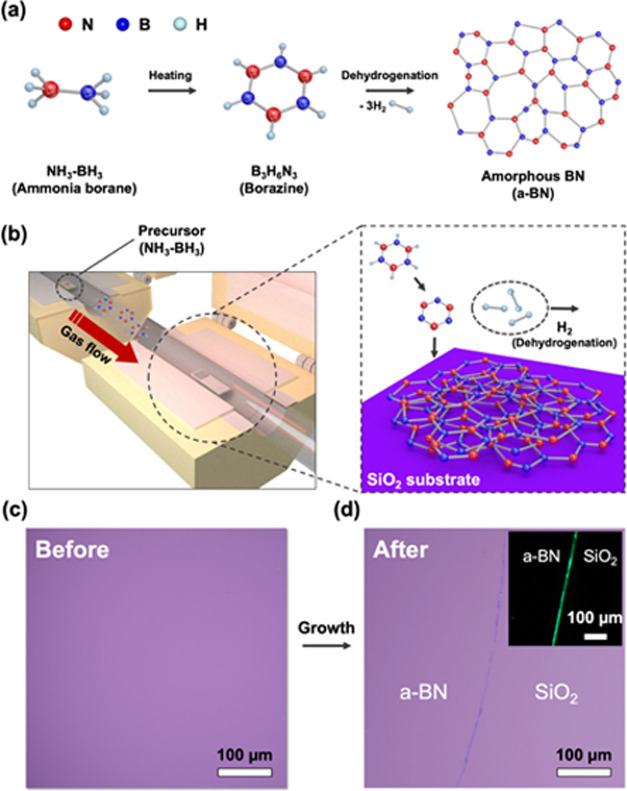
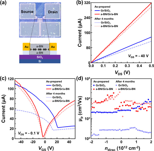
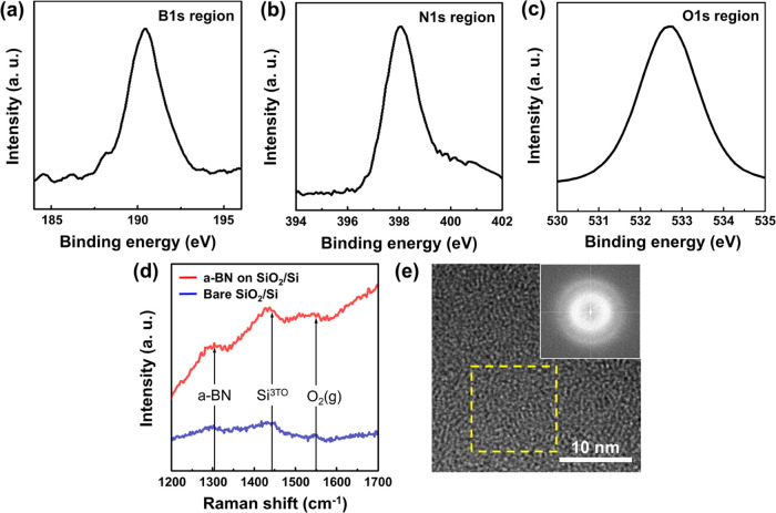
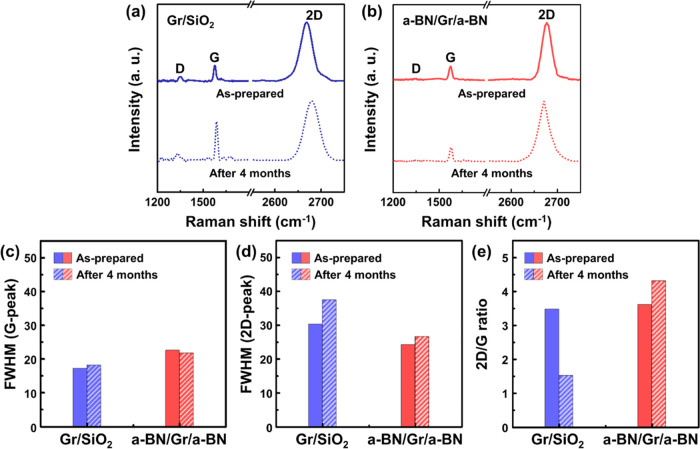
We successfully demonstrated the improvement and stabilization of the electrical properties of a graphene field effect transistor by fabricating a sandwiched amorphous boron nitride (a-BN)/graphene (Gr)/a-BN using a directly grown a-BN film. The a-BN film was grown low-pressure chemical vapor deposition (LPCVD) at a low growth temperature of 250 °C and applied as a protection layer in the sandwiched structure. Both structural and chemical states of the as-grown a-BN were verified by various spectroscopic and microscopic analyses. We analyzed the Raman spectra of Gr/SiO and a-BN/Gr/a-BN structures to determine the stability of the device under exposure to ambient air. Following exposure, the intensity of the 2D/G-peak ratio of Gr/SiO decreased and the position of the G and 2D peaks red-shifted due to the degradation of graphene. In contrast, the peak position of encapsulated graphene is almost unchanged. We also confirmed that the mobility of a-BN/Gr/a-BN structure is 17,941 cm/Vs. This synthetic strategy could provide a facile way to synthesize uniform a-BN film for encapsulating various van der Waals materials, which is beneficial for future applications in nanoelectronics.

摘要

我们成功地通过使用直接生长的非晶态氮化硼(a-BN)膜制造夹心结构的非晶态氮化硼(a-BN)/石墨烯(Gr)/非晶态氮化硼(a-BN),改善和稳定了石墨烯场效应晶体管的电学性能。该 a-BN 薄膜采用低压化学气相沉积(LPCVD)在 250°C 的低温下生长,并用作夹心结构中的保护层。通过各种光谱和显微镜分析验证了所生长的 a-BN 的结构和化学状态。我们分析了 Gr/SiO 和 a-BN/Gr/a-BN 结构的拉曼光谱,以确定器件在暴露于环境空气中的稳定性。暴露后,由于石墨烯的降解,Gr/SiO 中 2D/G-峰强度比降低,G 和 2D 峰的位置红移。相比之下,封装石墨烯的峰位置几乎不变。我们还证实,a-BN/Gr/a-BN 结构的迁移率为 17941cm/Vs。这种合成策略可以为封装各种范德华材料提供一种简便的方法来合成均匀的 a-BN 薄膜,这有利于未来在纳米电子学中的应用。

https://cdn.ncbi.nlm.nih.gov/pmc/blobs/8d19/9923684/04769301a6d9/am2c18706_0006.jpg
https://cdn.ncbi.nlm.nih.gov/pmc/blobs/8d19/9923684/7c82ab7dbc0d/am2c18706_0002.jpg
https://cdn.ncbi.nlm.nih.gov/pmc/blobs/8d19/9923684/ad9f2c056769/am2c18706_0003.jpg
https://cdn.ncbi.nlm.nih.gov/pmc/blobs/8d19/9923684/e39524e030ef/am2c18706_0004.jpg
https://cdn.ncbi.nlm.nih.gov/pmc/blobs/8d19/9923684/1ef56b92f76a/am2c18706_0005.jpg
https://cdn.ncbi.nlm.nih.gov/pmc/blobs/8d19/9923684/04769301a6d9/am2c18706_0006.jpg

相似文献

1
Low-Temperature Direct Growth of Amorphous Boron Nitride Films for High-Performance Nanoelectronic Device Applications.低温直接生长非晶氮化硼薄膜用于高性能纳电子器件应用。
ACS Appl Mater Interfaces. 2023 Feb 8;15(5):7274-7281. doi: 10.1021/acsami.2c18706. Epub 2023 Jan 31.
2
Atomic Layer Deposition of Layered Boron Nitride for Large-Area 2D Electronics.用于大面积二维电子器件的层状氮化硼的原子层沉积
ACS Appl Mater Interfaces. 2020 Aug 12;12(32):36688-36694. doi: 10.1021/acsami.0c07548. Epub 2020 Jul 29.
3
Low-Temperature Synthesis of Boron Nitride as a Large-Scale Passivation and Protection Layer for Two-Dimensional Materials and High-Performance Devices.作为二维材料和高性能器件的大规模钝化与保护层的氮化硼低温合成
ACS Appl Mater Interfaces. 2022 Jun 8;14(22):25984-25992. doi: 10.1021/acsami.2c02803. Epub 2022 May 23.
4
Van der Waals epitaxy and characterization of hexagonal boron nitride nanosheets on graphene.范德华外延法和石墨烯上六方氮化硼纳米片的特性研究。
Nanoscale Res Lett. 2014 Jul 28;9(1):367. doi: 10.1186/1556-276X-9-367. eCollection 2014.
5
High-mobility and air-stable single-layer WS2 field-effect transistors sandwiched between chemical vapor deposition-grown hexagonal BN films.夹在化学气相沉积生长的六方氮化硼薄膜之间的高迁移率且空气稳定的单层二硫化钨场效应晶体管。
Sci Rep. 2015 Jun 1;5:10699. doi: 10.1038/srep10699.
6
Highly Ordered Boron Nitride/Epigraphene Epitaxial Films on Silicon Carbide by Lateral Epitaxial Deposition.通过横向外延沉积在碳化硅上制备的高度有序的氮化硼/外延石墨烯外延薄膜。
ACS Nano. 2020 Oct 27;14(10):12962-12971. doi: 10.1021/acsnano.0c04164. Epub 2020 Oct 1.
7
Controlled Growth of Large-Area Uniform Multilayer Hexagonal Boron Nitride as an Effective 2D Substrate.大面积均匀多层六方氮化硼作为有效二维衬底的可控生长
ACS Nano. 2018 Jun 26;12(6):6236-6244. doi: 10.1021/acsnano.8b03055. Epub 2018 Jun 12.
8
Hexagonal Boron Nitride on III-V Compounds: A Review of the Synthesis and Applications.III-V族化合物上的六方氮化硼:合成与应用综述
Materials (Basel). 2022 Jun 22;15(13):4396. doi: 10.3390/ma15134396.
9
Direct growth of large-area graphene and boron nitride heterostructures by a co-segregation method.通过共偏析方法直接生长大面积石墨烯和氮化硼异质结。
Nat Commun. 2015 Mar 4;6:6519. doi: 10.1038/ncomms7519.
10
Chemical Interaction-Guided, Metal-Free Growth of Large-Area Hexagonal Boron Nitride on Silicon-Based Substrates.化学相互作用引导的、基于硅衬底的大面积六方氮化硼的无金属生长。
ACS Nano. 2017 May 23;11(5):4985-4994. doi: 10.1021/acsnano.7b01666. Epub 2017 May 1.

引用本文的文献

1
Recent Advances in Chemical Vapor Deposition of Hexagonal Boron Nitride on Insulating Substrates.绝缘衬底上六方氮化硼化学气相沉积的最新进展
Nanomaterials (Basel). 2025 Jul 8;15(14):1059. doi: 10.3390/nano15141059.
2
Low-Power Ternary Bipolar Memristor of Naturally Oxidized Porous TiCT MXene Flakes.自然氧化多孔TiCT MXene薄片的低功耗三值双极忆阻器
ACS Omega. 2025 Jun 19;10(25):27272-27278. doi: 10.1021/acsomega.5c02640. eCollection 2025 Jul 1.
3
Amorphous boron nitride: synthesis, properties and device application.非晶态氮化硼:合成、性质及器件应用。

本文引用的文献

1
One Pot Synthesis of Graphene through Microwave Assisted Liquid Exfoliation of Graphite in Different Solvents.通过微波辅助在不同溶剂中对石墨进行液相剥离一步法合成石墨烯
Molecules. 2022 Aug 7;27(15):5027. doi: 10.3390/molecules27155027.
2
Low-Temperature Synthesis of Boron Nitride as a Large-Scale Passivation and Protection Layer for Two-Dimensional Materials and High-Performance Devices.作为二维材料和高性能器件的大规模钝化与保护层的氮化硼低温合成
ACS Appl Mater Interfaces. 2022 Jun 8;14(22):25984-25992. doi: 10.1021/acsami.2c02803. Epub 2022 May 23.
3
Layer-engineered large-area exfoliation of graphene.
Nano Converg. 2025 May 2;12(1):22. doi: 10.1186/s40580-025-00486-1.
4
Stability and Reliability of van der Waals High-κ SrTiO Field-Effect Transistors with Small Hysteresis.具有小滞后的范德华高κ SrTiO场效应晶体管的稳定性和可靠性
ACS Nano. 2025 Apr 1;19(12):12288-12297. doi: 10.1021/acsnano.5c01145. Epub 2025 Mar 19.
5
2D amorphous solids for sub-nanometer scale devices.用于亚纳米级器件的二维非晶态固体。
Nano Converg. 2024 Nov 24;11(1):46. doi: 10.1186/s40580-024-00453-2.
6
Tailoring amorphous boron nitride for high-performance two-dimensional electronics.定制用于高性能二维电子学的非晶态氮化硼。
Nat Commun. 2024 May 13;15(1):4016. doi: 10.1038/s41467-024-48429-4.
7
Amorphous BN-Based Synaptic Device with High Performance in Neuromorphic Computing.用于神经形态计算的高性能非晶态氮化硼基突触器件。
Materials (Basel). 2023 Oct 15;16(20):6698. doi: 10.3390/ma16206698.
石墨烯的层状工程大面积剥离
Sci Adv. 2020 Oct 28;6(44). doi: 10.1126/sciadv.abc6601. Print 2020 Oct.
4
Atomically Thin Hexagonal Boron Nitride and Its Heterostructures.原子级薄的六方氮化硼及其异质结构
Adv Mater. 2021 Feb;33(6):e2000769. doi: 10.1002/adma.202000769. Epub 2020 Aug 16.
5
High-mobility junction field-effect transistor via graphene/MoS heterointerface.通过石墨烯/二硫化钼异质界面的高迁移率结型场效应晶体管。
Sci Rep. 2020 Aug 4;10(1):13101. doi: 10.1038/s41598-020-70038-6.
6
Atomic Layer Deposition of Layered Boron Nitride for Large-Area 2D Electronics.用于大面积二维电子器件的层状氮化硼的原子层沉积
ACS Appl Mater Interfaces. 2020 Aug 12;12(32):36688-36694. doi: 10.1021/acsami.0c07548. Epub 2020 Jul 29.
7
Insulators for 2D nanoelectronics: the gap to bridge.用于二维纳米电子学的绝缘体:有待弥合的差距。
Nat Commun. 2020 Jul 7;11(1):3385. doi: 10.1038/s41467-020-16640-8.
8
Synaptic Characteristics of Amorphous Boron Nitride-Based Memristors on a Highly Doped Silicon Substrate for Neuromorphic Engineering.用于神经形态工程的高掺杂硅衬底上基于非晶氮化硼的忆阻器的突触特性
ACS Appl Mater Interfaces. 2020 Jul 29;12(30):33908-33916. doi: 10.1021/acsami.0c07867. Epub 2020 Jul 15.
9
Ultralow-dielectric-constant amorphous boron nitride.超低介电常数非晶态氮化硼。
Nature. 2020 Jun;582(7813):511-514. doi: 10.1038/s41586-020-2375-9. Epub 2020 Jun 24.
10
Graphene-Based Mixed-Dimensional van der Waals Heterostructures for Advanced Optoelectronics.基于石墨烯的混合维度范德华异质结构用于先进光电子学。
Adv Mater. 2019 Sep;31(37):e1806411. doi: 10.1002/adma.201806411. Epub 2019 Jul 10.