• 文献检索
  • 文档翻译
  • 深度研究
  • 学术资讯
  • Suppr Zotero 插件Zotero 插件
  • 邀请有礼
  • 套餐&价格
  • 历史记录
应用&插件
Suppr Zotero 插件Zotero 插件浏览器插件Mac 客户端Windows 客户端微信小程序
定价
高级版会员购买积分包购买API积分包
服务
文献检索文档翻译深度研究API 文档MCP 服务
关于我们
关于 Suppr公司介绍联系我们用户协议隐私条款
关注我们

Suppr 超能文献

核心技术专利:CN118964589B侵权必究
粤ICP备2023148730 号-1Suppr @ 2026

文献检索

告别复杂PubMed语法,用中文像聊天一样搜索,搜遍4000万医学文献。AI智能推荐,让科研检索更轻松。

立即免费搜索

文件翻译

保留排版,准确专业,支持PDF/Word/PPT等文件格式,支持 12+语言互译。

免费翻译文档

深度研究

AI帮你快速写综述,25分钟生成高质量综述,智能提取关键信息,辅助科研写作。

立即免费体验

具有低温溶液处理的二硒化钨的高迁移率柔性晶体管。

High-Mobility Flexible Transistors with Low-Temperature Solution-Processed Tungsten Dichalcogenides.

机构信息

School of Physics, CRANN & AMBER Research Centres, Trinity College Dublin, Dublin D02 E8C0, Ireland.

出版信息

ACS Nano. 2023 Feb 14;17(3):2912-2922. doi: 10.1021/acsnano.2c11319. Epub 2023 Jan 31.

DOI:10.1021/acsnano.2c11319
PMID:36720070
原文链接:https://pmc.ncbi.nlm.nih.gov/articles/PMC9933598/
Abstract

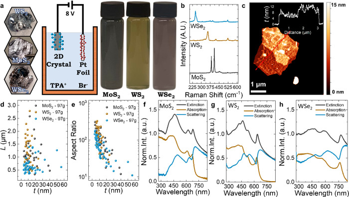
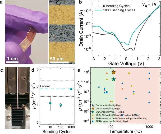
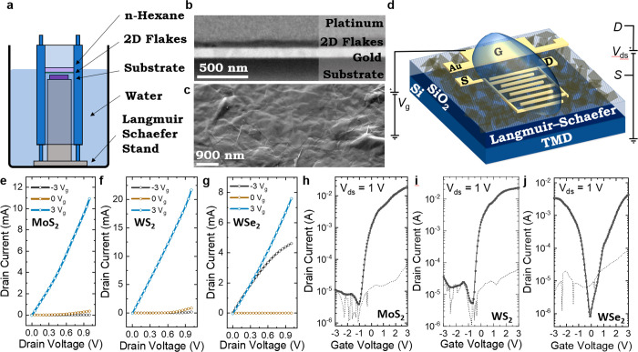
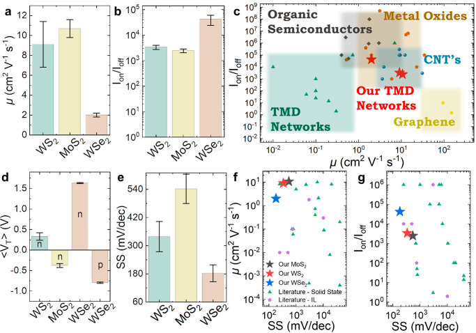
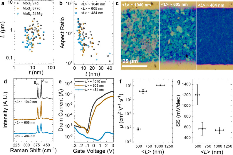
The investigation of high-mobility two-dimensional (2D) flakes beyond molybdenum disulfide (MoS) will be necessary to create a library of high-mobility solution-processed networks that conform to substrates and remain functional over thousands of bending cycles. Here we report electrochemical exfoliation of large-aspect-ratio (>100) semiconducting flakes of tungsten diselenide (WSe) and tungsten disulfide (WS) as well as MoS as a comparison. We use Langmuir-Schaefer coating to achieve highly aligned and conformal flake networks, with minimal mesoporosity (∼2-5%), at low processing temperatures (120 °C) and without acid treatments. This allows us to fabricate electrochemical transistors in ambient air, achieving average mobilities of μ ≈ 11 cm V s, μ ≈ 9 cm V s, and μ ≈ 2 cm V s with a current on/off ratios of / ≈ 2.6 × 10, 3.4 × 10, and 4.2 × 10 for MoS, WS, and WSe, respectively. Moreover, our transistors display threshold voltages near ∼0.4 V with subthreshold slopes as low as 182 mV/dec, which are essential factors in maintaining power efficiency and represent a 1 order of magnitude improvement in the state of the art. Furthermore, the performance of our WSe transistors is maintained on polyethylene terephthalate (PET) even after 1000 bending cycles at 1% strain.

摘要

为了创建一个符合衬底且能在数千个弯曲循环中保持功能的高迁移率溶液处理网络库,除了二硫化钼(MoS)之外,对二维(2D)高迁移率薄片的研究将是必要的。在这里,我们报告了电化学剥离大纵横比(>100)的半导体二硒化钨(WSe)和二硫化钨(WS)以及 MoS 薄片,作为比较。我们使用 Langmuir-Schaefer 涂层来实现高度对齐和共形的薄片网络,在低处理温度(120°C)和无酸处理的情况下,具有最小的介孔率(约 2-5%)。这使我们能够在环境空气中制造电化学晶体管,实现平均迁移率μ≈11 cm V s,μ≈9 cm V s,μ≈2 cm V s,电流比为/≈2.6×10、3.4×10和 4.2×10,分别对应 MoS、WS 和 WSe。此外,我们的晶体管显示出接近约 0.4 V 的阈值电压,亚阈值斜率低至 182 mV/dec,这是保持功率效率的重要因素,代表了现有技术的一个数量级的改进。此外,我们的 WSe 晶体管在聚对苯二甲酸乙二醇酯(PET)上的性能在 1%应变下经过 1000 次弯曲循环后仍能保持。

https://cdn.ncbi.nlm.nih.gov/pmc/blobs/47f2/9933598/5a359d8e3643/nn2c11319_0005.jpg
https://cdn.ncbi.nlm.nih.gov/pmc/blobs/47f2/9933598/ea6defd28408/nn2c11319_0001.jpg
https://cdn.ncbi.nlm.nih.gov/pmc/blobs/47f2/9933598/c0d524485485/nn2c11319_0002.jpg
https://cdn.ncbi.nlm.nih.gov/pmc/blobs/47f2/9933598/f88622bd614d/nn2c11319_0003.jpg
https://cdn.ncbi.nlm.nih.gov/pmc/blobs/47f2/9933598/d181fc8c2b10/nn2c11319_0004.jpg
https://cdn.ncbi.nlm.nih.gov/pmc/blobs/47f2/9933598/5a359d8e3643/nn2c11319_0005.jpg

相似文献

1
High-Mobility Flexible Transistors with Low-Temperature Solution-Processed Tungsten Dichalcogenides.具有低温溶液处理的二硒化钨的高迁移率柔性晶体管。
ACS Nano. 2023 Feb 14;17(3):2912-2922. doi: 10.1021/acsnano.2c11319. Epub 2023 Jan 31.
2
Knot Architecture for Biocompatible and Semiconducting 2D Electronic Fiber Transistors.用于生物相容性和半导体二维电子纤维晶体管的结结构
Small Methods. 2024 Oct;8(10):e2301654. doi: 10.1002/smtd.202301654. Epub 2024 Apr 11.
3
High-Performance WSe2 Field-Effect Transistors via Controlled Formation of In-Plane Heterojunctions.通过控制平面内异质结的形成来实现高性能 WSe2 场效应晶体管。
ACS Nano. 2016 May 24;10(5):5153-60. doi: 10.1021/acsnano.6b00527. Epub 2016 May 9.
4
Reversible Semiconducting-to-Metallic Phase Transition in Chemical Vapor Deposition Grown Monolayer WSe2 and Applications for Devices.化学气相沉积生长的单层 WSe2 的可逆半导体-金属相转变及器件应用。
ACS Nano. 2015 Jul 28;9(7):7383-91. doi: 10.1021/acsnano.5b02399. Epub 2015 Jun 30.
5
Toward Scalable Electrochemical Exfoliation of Molybdenum Disulfide Powder through an Accessible Electrode Design.通过可及电极设计实现二硫化钼粉末的可扩展电化学剥离
Small Methods. 2025 Jan;9(1):e2400298. doi: 10.1002/smtd.202400298. Epub 2024 Jul 17.
6
Synthesis of Large-Area Tungsten Disulfide Films on Pre-Reduced Tungsten Suboxide Substrates.大面积二硫化钨薄膜在预还原五氧化二钨基底上的合成。
ACS Appl Mater Interfaces. 2017 Dec 13;9(49):43021-43029. doi: 10.1021/acsami.7b12151. Epub 2017 Nov 28.
7
Mechanical Properties of Atomically Thin Tungsten Dichalcogenides: WS, WSe, and WTe.原子级薄二硫化钨的力学性能:WS、WSe和WTe
ACS Nano. 2021 Feb 23;15(2):2600-2610. doi: 10.1021/acsnano.0c07430. Epub 2021 Jan 27.
8
High-Performance Solution-Processed 2D P-Type WSe Transistors and Circuits through Molecular Doping.通过分子掺杂实现高性能溶液处理二维 P 型 WSe 晶体管和电路。
Adv Mater. 2023 Feb;35(7):e2208934. doi: 10.1002/adma.202208934. Epub 2022 Dec 16.
9
Facile Exfoliation for High-Quality Molybdenum Disulfide Nanoflakes and Relevant Field-Effect Transistors Developed With Thermal Treatment.通过热处理实现高质量二硫化钼纳米片的简便剥离及相关场效应晶体管的制备
Front Chem. 2021 Apr 26;9:650901. doi: 10.3389/fchem.2021.650901. eCollection 2021.
10
Van der Waals contacts between three-dimensional metals and two-dimensional semiconductors.三维金属与二维半导体之间的范德华接触。
Nature. 2019 Apr;568(7750):70-74. doi: 10.1038/s41586-019-1052-3. Epub 2019 Mar 27.

引用本文的文献

1
Solution-processed negative gauge factor PtSe strain sensors.溶液处理的负应变系数PtSe应变传感器。
Nanoscale. 2025 Jul 22. doi: 10.1039/d5nr01217a.
2
Solution-Processable Electronic-Grade 2D WTe Enabled by Synergistic Dual Ammonium Intercalation.通过协同双铵插层实现的可溶液加工电子级二维WTe₂
ACS Nano. 2025 Apr 15;19(14):14309-14317. doi: 10.1021/acsnano.5c01224. Epub 2025 Apr 2.
3
Carrier Multiplication and Photoexcited Many-Body States in Solution-Processed 2H-MoSe.溶液处理的2H-MoSe₂中的载流子倍增与光激发多体状态

本文引用的文献

1
High Performance Semiconducting Nanosheets a Scalable Powder-Based Electrochemical Exfoliation Technique.高性能半导体纳米片:一种基于粉末的可扩展电化学剥离技术
ACS Nano. 2022 Apr 26;16(4):5719-5730. doi: 10.1021/acsnano.1c10739. Epub 2022 Mar 15.
2
Highly Conductive Networks of Silver Nanosheets.银纳米片的高导电网络
Small. 2022 Apr;18(14):e2105996. doi: 10.1002/smll.202105996. Epub 2022 Feb 26.
3
Low Subthreshold Slope AlGaN/GaN MOS-HEMT with Spike-Annealed HfO Gate Dielectric.采用尖峰退火HfO栅介质的低亚阈值斜率AlGaN/GaN MOS-HEMT
ACS Nano. 2025 Mar 18;19(10):10347-10358. doi: 10.1021/acsnano.4c18254. Epub 2025 Mar 6.
4
Exfoliated Molybdenum Disulfide Nanosheet Networks as Sensing Materials for Nitrogen Dioxide Detection.用于二氧化氮检测的剥离型二硫化钼纳米片网络作为传感材料
ACS Appl Nano Mater. 2025 Jan 24;8(5):2141-2152. doi: 10.1021/acsanm.4c05066. eCollection 2025 Feb 7.
5
Printed Lithography of Graphene-Perovskite Quantum Dot Hybrid Photodetectors on Paper Substrates.纸质基底上石墨烯-钙钛矿量子点混合光电探测器的印刷光刻技术
ACS Appl Mater Interfaces. 2025 Jan 29;17(4):6716-6727. doi: 10.1021/acsami.4c18102. Epub 2025 Jan 20.
6
Layer-by-layer assembly yields thin graphene films with near theoretical conductivity.逐层组装可产生具有接近理论电导率的薄石墨烯薄膜。
NPJ 2D Mater Appl. 2025;9(1):2. doi: 10.1038/s41699-025-00525-9. Epub 2025 Jan 8.
7
Using Electrical Impedance Spectroscopy to Separately Quantify the Effect of Strain on Nanosheet and Junction Resistance in Printed Nanosheet Networks.使用电阻抗光谱法分别量化应变对印刷纳米片网络中纳米片和结电阻的影响。
Small. 2025 Feb;21(5):e2406864. doi: 10.1002/smll.202406864. Epub 2024 Dec 18.
8
Inert Liquid Exfoliation and Langmuir-Type Thin Film Deposition of Semimetallic Metal Diborides.半金属二硼化物的惰性液体剥离及朗缪尔型薄膜沉积
ACS Nano. 2024 Oct 22;18(42):28596-28608. doi: 10.1021/acsnano.4c04626. Epub 2024 Oct 9.
9
Two-dimensional fully ferroelectric-gated hybrid computing-in-memory hardware for high-precision and energy-efficient dynamic tracking.用于高精度和节能动态跟踪的二维全铁电门控混合计算内存硬件。
Sci Adv. 2024 Sep 6;10(36):eadp0174. doi: 10.1126/sciadv.adp0174. Epub 2024 Sep 4.
10
Toward Scalable Electrochemical Exfoliation of Molybdenum Disulfide Powder through an Accessible Electrode Design.通过可及电极设计实现二硫化钼粉末的可扩展电化学剥离
Small Methods. 2025 Jan;9(1):e2400298. doi: 10.1002/smtd.202400298. Epub 2024 Jul 17.
Micromachines (Basel). 2021 Nov 25;12(12):1441. doi: 10.3390/mi12121441.
4
All-Solution-Processed Van der Waals Heterostructures for Wafer-Scale Electronics.用于晶圆级电子学的全溶液处理范德华异质结构
Adv Mater. 2022 Mar;34(12):e2106110. doi: 10.1002/adma.202106110. Epub 2022 Feb 8.
5
Area-Selective Chemical Doping on Solution-Processed MoS Thin-Film for Multi-Valued Logic Gates.用于多值逻辑门的溶液处理MoS薄膜上的区域选择性化学掺杂
Nano Lett. 2022 Jan 26;22(2):570-577. doi: 10.1021/acs.nanolett.1c02947. Epub 2021 Nov 15.
6
Fibre electronics: towards scaled-up manufacturing of integrated e-textile systems.纤维电子学:迈向集成电子纺织系统的规模化制造。
Nanoscale. 2021 Aug 14;13(30):12818-12847. doi: 10.1039/d1nr02061g. Epub 2021 Jul 22.
7
Quantification and Healing of Defects in Atomically Thin Molybdenum Disulfide: Beyond the Controlled Creation of Atomic Defects.原子级薄二硫化钼中缺陷的量化与修复:超越原子缺陷的可控生成
ACS Nano. 2021 Jun 22;15(6):9658-9669. doi: 10.1021/acsnano.0c10897. Epub 2021 Mar 23.
8
Covalently interconnected transition metal dichalcogenide networks via defect engineering for high-performance electronic devices.通过缺陷工程实现共价互连的过渡金属二硫属化物网络用于高性能电子器件。
Nat Nanotechnol. 2021 May;16(5):592-598. doi: 10.1038/s41565-021-00857-9. Epub 2021 Feb 25.
9
Benchmarking monolayer MoS and WS field-effect transistors.基准测试单层MoS和WS场效应晶体管。
Nat Commun. 2021 Jan 29;12(1):693. doi: 10.1038/s41467-020-20732-w.
10
One-step synthesis of single-site vanadium substitution in 1T-WS monolayers for enhanced hydrogen evolution catalysis.一步合成单原子钒取代的1T-WS单层用于增强析氢催化
Nat Commun. 2021 Jan 29;12(1):709. doi: 10.1038/s41467-021-20951-9.