• 文献检索
  • 文档翻译
  • 深度研究
  • 学术资讯
  • Suppr Zotero 插件Zotero 插件
  • 邀请有礼
  • 套餐&价格
  • 历史记录
应用&插件
Suppr Zotero 插件Zotero 插件浏览器插件Mac 客户端Windows 客户端微信小程序
定价
高级版会员购买积分包购买API积分包
服务
文献检索文档翻译深度研究API 文档MCP 服务
关于我们
关于 Suppr公司介绍联系我们用户协议隐私条款
关注我们

Suppr 超能文献

核心技术专利:CN118964589B侵权必究
粤ICP备2023148730 号-1Suppr @ 2026

文献检索

告别复杂PubMed语法,用中文像聊天一样搜索,搜遍4000万医学文献。AI智能推荐,让科研检索更轻松。

立即免费搜索

文件翻译

保留排版,准确专业,支持PDF/Word/PPT等文件格式,支持 12+语言互译。

免费翻译文档

深度研究

AI帮你快速写综述,25分钟生成高质量综述,智能提取关键信息,辅助科研写作。

立即免费体验

石墨烯晶体管中的共振隧穿和负微分电导。

Resonant tunnelling and negative differential conductance in graphene transistors.

机构信息

School of Physics and Astronomy, University of Manchester, Manchester M13 9PL, UK.

出版信息

Nat Commun. 2013;4:1794. doi: 10.1038/ncomms2817.

DOI:10.1038/ncomms2817
PMID:23653206
原文链接:https://pmc.ncbi.nlm.nih.gov/articles/PMC3644101/
Abstract

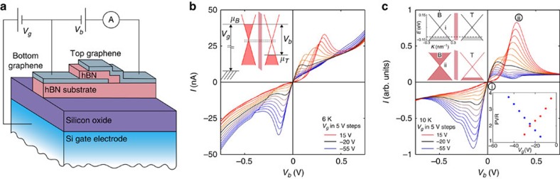
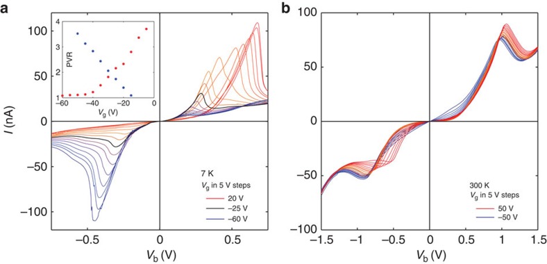
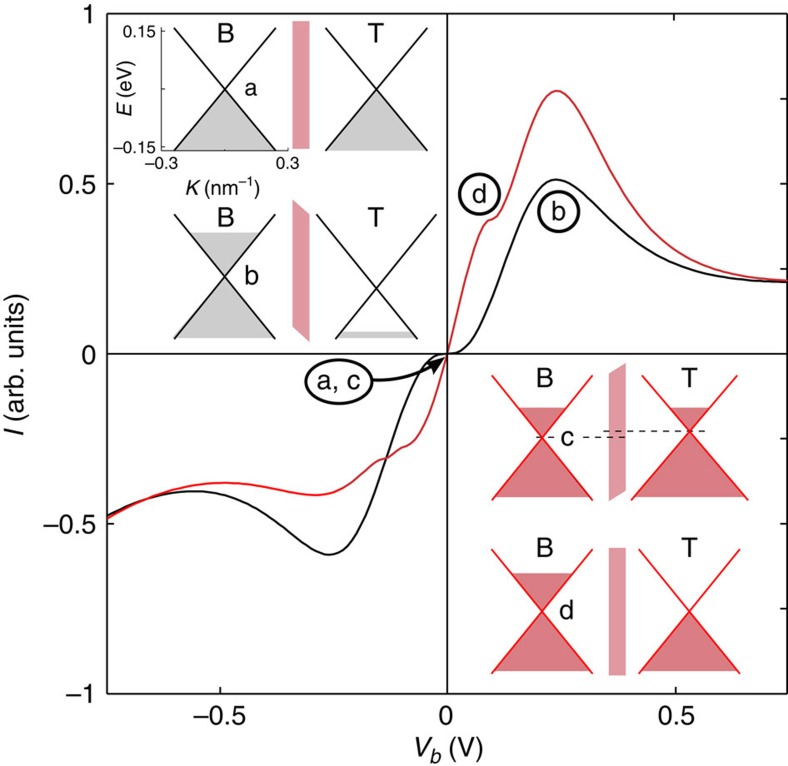
The chemical stability of graphene and other free-standing two-dimensional crystals means that they can be stacked in different combinations to produce a new class of functional materials, designed for specific device applications. Here we report resonant tunnelling of Dirac fermions through a boron nitride barrier, a few atomic layers thick, sandwiched between two graphene electrodes. The resonance occurs when the electronic spectra of the two electrodes are aligned. The resulting negative differential conductance in the device characteristics persists up to room temperature and is gate voltage-tuneable due to graphene's unique Dirac-like spectrum. Although conventional resonant tunnelling devices comprising a quantum well sandwiched between two tunnel barriers are tens of nanometres thick, the tunnelling carriers in our devices cross only a few atomic layers, offering the prospect of ultra-fast transit times. This feature, combined with the multi-valued form of the device characteristics, has potential for applications in high-frequency and logic devices.

摘要

石墨烯和其他独立二维晶体的化学稳定性意味着它们可以以不同的组合堆叠,从而产生一类新的功能性材料,专门针对特定的器件应用而设计。在这里,我们报告了狄拉克费米子通过硼氮层间的共振隧穿,该硼氮层厚几原子层,夹在两个石墨烯电极之间。当两个电极的电子谱对齐时,就会发生共振。该器件特性中的负微分电导在室温下持续存在,并且由于石墨烯独特的类狄拉克谱,可以通过栅极电压进行调节。尽管传统的共振隧穿器件包括夹在两个隧道势垒之间的量子阱,厚度为数十纳米,但我们的器件中的隧穿载流子仅穿过几个原子层,从而提供了超快速传输时间的可能性。这种特性,加上器件特性的多值形式,在高频和逻辑器件中有潜在的应用。

https://cdn.ncbi.nlm.nih.gov/pmc/blobs/4f1b/3644101/a650de9d81e7/ncomms2817-f3.jpg
https://cdn.ncbi.nlm.nih.gov/pmc/blobs/4f1b/3644101/0ce04e274c2c/ncomms2817-f1.jpg
https://cdn.ncbi.nlm.nih.gov/pmc/blobs/4f1b/3644101/8e89321c20e0/ncomms2817-f2.jpg
https://cdn.ncbi.nlm.nih.gov/pmc/blobs/4f1b/3644101/a650de9d81e7/ncomms2817-f3.jpg
https://cdn.ncbi.nlm.nih.gov/pmc/blobs/4f1b/3644101/0ce04e274c2c/ncomms2817-f1.jpg
https://cdn.ncbi.nlm.nih.gov/pmc/blobs/4f1b/3644101/8e89321c20e0/ncomms2817-f2.jpg
https://cdn.ncbi.nlm.nih.gov/pmc/blobs/4f1b/3644101/a650de9d81e7/ncomms2817-f3.jpg

相似文献

1
Resonant tunnelling and negative differential conductance in graphene transistors.石墨烯晶体管中的共振隧穿和负微分电导。
Nat Commun. 2013;4:1794. doi: 10.1038/ncomms2817.
2
Twist-controlled resonant tunnelling in graphene/boron nitride/graphene heterostructures.扭曲控制的石墨烯/氮化硼/石墨烯异质结构中的共振隧穿。
Nat Nanotechnol. 2014 Oct;9(10):808-13. doi: 10.1038/nnano.2014.187. Epub 2014 Sep 7.
3
Negative differential resistance in boron nitride graphene heterostructures: physical mechanisms and size scaling analysis.氮化硼-石墨烯异质结构中的负微分电阻:物理机制与尺寸缩放分析
Sci Rep. 2015 May 20;5:10712. doi: 10.1038/srep10712.
4
Robust Quantum Oscillation of Dirac Fermions in a Single-Defect Resonant Transistor.单缺陷共振晶体管中狄拉克费米子的稳健量子振荡
ACS Nano. 2021 Dec 28;15(12):20013-20019. doi: 10.1021/acsnano.1c07613. Epub 2021 Nov 29.
5
Designer Dirac fermions and topological phases in molecular graphene.分子石墨中的设计狄拉克费米子和拓扑相。
Nature. 2012 Mar 14;483(7389):306-10. doi: 10.1038/nature10941.
6
Resonant Light Emission from Graphene/Hexagonal Boron Nitride/Graphene Tunnel Junctions.石墨烯/六方氮化硼/石墨烯隧道结的共振光发射
Nano Lett. 2021 Oct 13;21(19):8332-8339. doi: 10.1021/acs.nanolett.1c02913. Epub 2021 Oct 4.
7
Cloning of Dirac fermions in graphene superlattices.在石墨烯超晶格中狄拉克费米子的克隆。
Nature. 2013 May 30;497(7451):594-7. doi: 10.1038/nature12187. Epub 2013 May 15.
8
Effects of Electrode Layer Band Structure on the Performance of Multilayer Graphene-hBN-Graphene Interlayer Tunnel Field Effect Transistors.电极层能带结构对多层石墨烯-hBN-石墨烯层间隧道场效应晶体管性能的影响。
Nano Lett. 2016 Aug 10;16(8):4975-81. doi: 10.1021/acs.nanolett.6b01646. Epub 2016 Jul 20.
9
Phonon-Assisted Resonant Tunneling of Electrons in Graphene-Boron Nitride Transistors.石墨烯-氮化硼晶体管中电子的声子辅助共振隧穿
Phys Rev Lett. 2016 May 6;116(18):186603. doi: 10.1103/PhysRevLett.116.186603. Epub 2016 May 5.
10
Detection of graphene's divergent orbital diamagnetism at the Dirac point.在狄拉克点检测石墨烯的发散轨道抗磁性。
Science. 2021 Dec 10;374(6573):1399-1402. doi: 10.1126/science.abf9396. Epub 2021 Dec 9.

引用本文的文献

1
Toward high-current-density and high-frequency graphene resonant tunneling transistors.迈向高电流密度和高频石墨烯共振隧穿晶体管。
Nat Commun. 2025 May 23;16(1):4805. doi: 10.1038/s41467-025-58720-7.
2
Probing Electronic Band Structure of Monolayer MoS in Gate-Controlled Resonant Tunneling Diodes.探测栅极控制共振隧穿二极管中单层二硫化钼的电子能带结构
ACS Appl Mater Interfaces. 2025 Apr 30;17(17):25915-25921. doi: 10.1021/acsami.4c21712. Epub 2025 Apr 15.
3
Nanometer-Scale 1D Negative Differential Resistance Channels in Van Der Waals Layers.

本文引用的文献

1
Vertical field-effect transistor based on graphene-WS2 heterostructures for flexible and transparent electronics.基于石墨烯-WS2 异质结构的垂直场效应晶体管,用于柔性透明电子学。
Nat Nanotechnol. 2013 Feb;8(2):100-3. doi: 10.1038/nnano.2012.224. Epub 2012 Dec 23.
2
Graphene and boron nitride lateral heterostructures for atomically thin circuitry.用于原子薄电路的石墨烯和氮化硼范德华异质结
Nature. 2012 Aug 30;488(7413):627-32. doi: 10.1038/nature11408.
3
Cross-sectional imaging of individual layers and buried interfaces of graphene-based heterostructures and superlattices.
范德华层中的纳米级一维负微分电阻通道
Adv Sci (Weinh). 2025 Jan;12(2):e2408090. doi: 10.1002/advs.202408090. Epub 2024 Nov 13.
4
Transport in a Two-Channel Nanotransistor Device with Lateral Resonant Tunneling.具有横向共振隧穿的双通道纳米晶体管器件中的输运
Micromachines (Basel). 2024 Oct 19;15(10):1270. doi: 10.3390/mi15101270.
5
A hot-emitter transistor based on stimulated emission of heated carriers.基于热载流子受激辐射的热发射器晶体管。
Nature. 2024 Aug;632(8026):782-787. doi: 10.1038/s41586-024-07785-3. Epub 2024 Aug 14.
6
Large negative differential conductance and its transformation in a single radical molecule.单个自由基分子中的大负微分电导及其转变
Chem Sci. 2024 Jun 3;15(28):10989-10996. doi: 10.1039/d4sc01782j. eCollection 2024 Jul 17.
7
Quantum Graphene Asymmetric Devices for Harvesting Electromagnetic Energy.用于收集电磁能量的量子石墨烯非对称器件。
Nanomaterials (Basel). 2024 Jun 28;14(13):1114. doi: 10.3390/nano14131114.
8
Harnessing Quantum Capacitance in 2D Material/Molecular Layer Junctions for Novel Electronic Device Functionality.利用二维材料/分子层结中的量子电容实现新型电子器件功能。
Nanomaterials (Basel). 2024 Jun 3;14(11):972. doi: 10.3390/nano14110972.
9
Time, momentum, and energy resolved pump-probe tunneling spectroscopy of two-dimensional electron systems.二维电子系统的时间、动量和能量分辨泵浦-探测隧穿光谱学。
Nat Commun. 2023 Nov 17;14(1):7440. doi: 10.1038/s41467-023-43268-1.
10
Toward High-Peak-to-Valley-Ratio Graphene Resonant Tunneling Diodes.迈向高峰谷比石墨烯共振隧穿二极管
Nano Lett. 2023 Sep 13;23(17):8132-8139. doi: 10.1021/acs.nanolett.3c02281. Epub 2023 Sep 5.
基于石墨烯的异质结构和超晶格的各层和埋层界面的横截面成像。
Nat Mater. 2012 Sep;11(9):764-7. doi: 10.1038/nmat3386. Epub 2012 Jul 29.
4
Position effects of single vacancy on transport properties of single layer armchair h-BNC heterostructure.单层扶手椅 h-BNC 杂化结构中单空位对输运性质的位置效应。
Phys Chem Chem Phys. 2012 Aug 28;14(32):11478-83. doi: 10.1039/c2cp41210a. Epub 2012 Jul 17.
5
Graphene barristor, a triode device with a gate-controlled Schottky barrier.石墨烯条形电阻器,一种具有栅控肖特基势垒的三端器件。
Science. 2012 Jun 1;336(6085):1140-3. doi: 10.1126/science.1220527. Epub 2012 May 17.
6
Electron tunneling through ultrathin boron nitride crystalline barriers.电子隧穿超薄氮化硼晶体势垒。
Nano Lett. 2012 Mar 14;12(3):1707-10. doi: 10.1021/nl3002205. Epub 2012 Mar 1.
7
Lateral graphene-hBCN heterostructures as a platform for fully two-dimensional transistors.侧向石墨烯- hBCN 杂化结构作为全二维晶体管的平台。
ACS Nano. 2012 Mar 27;6(3):2642-8. doi: 10.1021/nn300019b. Epub 2012 Mar 2.
8
Three-terminal graphene negative differential resistance devices.三端石墨烯负微分电阻器件。
ACS Nano. 2012 Mar 27;6(3):2610-6. doi: 10.1021/nn205106z. Epub 2012 Feb 16.
9
Field-effect tunneling transistor based on vertical graphene heterostructures.基于垂直石墨烯异质结构的场效应隧穿晶体管。
Science. 2012 Feb 24;335(6071):947-50. doi: 10.1126/science.1218461. Epub 2012 Feb 2.
10
Correlated charged impurity scattering in graphene.石墨烯中的关联带电杂质散射。
Phys Rev Lett. 2011 Nov 11;107(20):206601. doi: 10.1103/PhysRevLett.107.206601. Epub 2011 Nov 7.