Department of Materials Science and Engineering, University of Wisconsin-Madison, 1509 University Avenue, Madison, WI 53706, USA.
Department of Engineering Physics, University of Wisconsin-Platteville, 1 University Plaza, Platteville, WI 53818, USA.
Sci Adv. 2016 Sep 2;2(9):e1601240. doi: 10.1126/sciadv.1601240. eCollection 2016 Sep.
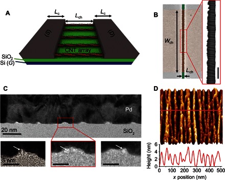
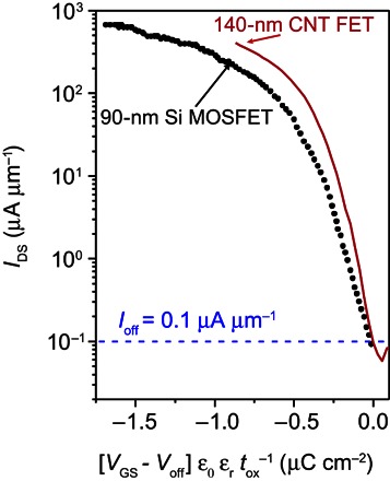
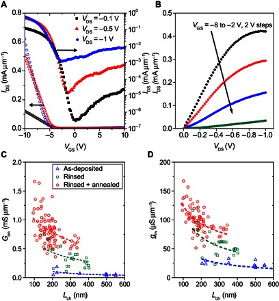
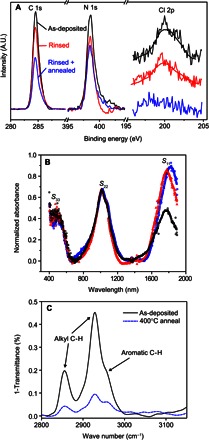
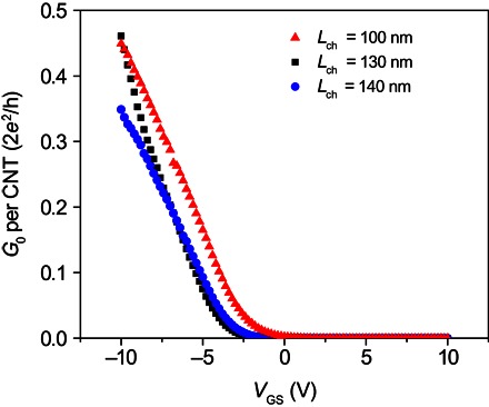
Carbon nanotubes (CNTs) are tantalizing candidates for semiconductor electronics because of their exceptional charge transport properties and one-dimensional electrostatics. Ballistic transport approaching the quantum conductance limit of 2G 0 = 4e (2)/h has been achieved in field-effect transistors (FETs) containing one CNT. However, constraints in CNT sorting, processing, alignment, and contacts give rise to nonidealities when CNTs are implemented in densely packed parallel arrays such as those needed for technology, resulting in a conductance per CNT far from 2G 0. The consequence has been that, whereas CNTs are ultimately expected to yield FETs that are more conductive than conventional semiconductors, CNTs, instead, have underperformed channel materials, such as Si, by sixfold or more. We report quasi-ballistic CNT array FETs at a density of 47 CNTs μm(-1), fabricated through a combination of CNT purification, solution-based assembly, and CNT treatment. The conductance is as high as 0.46 G 0 per CNT. In parallel, the conductance of the arrays reaches 1.7 mS μm(-1), which is seven times higher than the previous state-of-the-art CNT array FETs made by other methods. The saturated on-state current density is as high as 900 μA μm(-1) and is similar to or exceeds that of Si FETs when compared at and equivalent gate oxide thickness and at the same off-state current density. The on-state current density exceeds that of GaAs FETs as well. This breakthrough in CNT array performance is a critical advance toward the exploitation of CNTs in logic, high-speed communications, and other semiconductor electronics technologies.
碳纳米管(CNTs)作为半导体电子学中极具吸引力的候选材料,是因为它们具有出色的电荷输运特性和一维静电特性。在包含一个 CNT 的场效应晶体管(FET)中,已经实现了接近量子电导极限 2G0=4e(2)/h 的弹道输运。然而,在 CNT 进行排序、处理、对齐和接触时,由于受到限制,当 CNT 被用于需要技术的密集平行排列(例如,需要技术的密集平行排列)时,会产生不理想的情况,从而导致每个 CNT 的电导远低于 2G0。其结果是,尽管 CNT 最终有望产生比传统半导体更具导电性的 FET,但 CNT 表现却逊于通道材料,例如 Si,相差六倍或更多。我们报告了一种密度为 47 CNTs μm(-1) 的准弹道 CNT 阵列 FET,该 FET 通过 CNT 纯化、基于溶液的组装和 CNT 处理的组合来制造。电导高达 0.46 G0 每 CNT。与此同时,该阵列的电导达到 1.7 mS μm(-1),比以前通过其他方法制造的 CNT 阵列 FET 高七倍。饱和导通电流密度高达 900 μA μm(-1),当与等效栅氧化层厚度和相同的关断电流密度相比时,与 Si FET 相似或超过 Si FET。导通电流密度也超过了 GaAs FET。这种 CNT 阵列性能的突破是在逻辑、高速通信和其他半导体电子技术中利用 CNT 的关键进展。