• 文献检索
  • 文档翻译
  • 深度研究
  • 学术资讯
  • Suppr Zotero 插件Zotero 插件
  • 邀请有礼
  • 套餐&价格
  • 历史记录
应用&插件
Suppr Zotero 插件Zotero 插件浏览器插件Mac 客户端Windows 客户端微信小程序
定价
高级版会员购买积分包购买API积分包
服务
文献检索文档翻译深度研究API 文档MCP 服务
关于我们
关于 Suppr公司介绍联系我们用户协议隐私条款
关注我们

Suppr 超能文献

核心技术专利:CN118964589B侵权必究
粤ICP备2023148730 号-1Suppr @ 2026

文献检索

告别复杂PubMed语法,用中文像聊天一样搜索,搜遍4000万医学文献。AI智能推荐,让科研检索更轻松。

立即免费搜索

文件翻译

保留排版,准确专业,支持PDF/Word/PPT等文件格式,支持 12+语言互译。

免费翻译文档

深度研究

AI帮你快速写综述,25分钟生成高质量综述,智能提取关键信息,辅助科研写作。

立即免费体验

基于 CMOS 的碳纳米管传输晶体管逻辑集成电路。

CMOS-based carbon nanotube pass-transistor logic integrated circuits.

机构信息

Key Laboratory for the Physics and Chemistry of Nanodevices, and Department of Electronics, Peking University, Beijing 100871, China.

出版信息

Nat Commun. 2012 Feb 14;3:677. doi: 10.1038/ncomms1682.

DOI:10.1038/ncomms1682
PMID:22334080
原文链接:https://pmc.ncbi.nlm.nih.gov/articles/PMC3293427/
Abstract

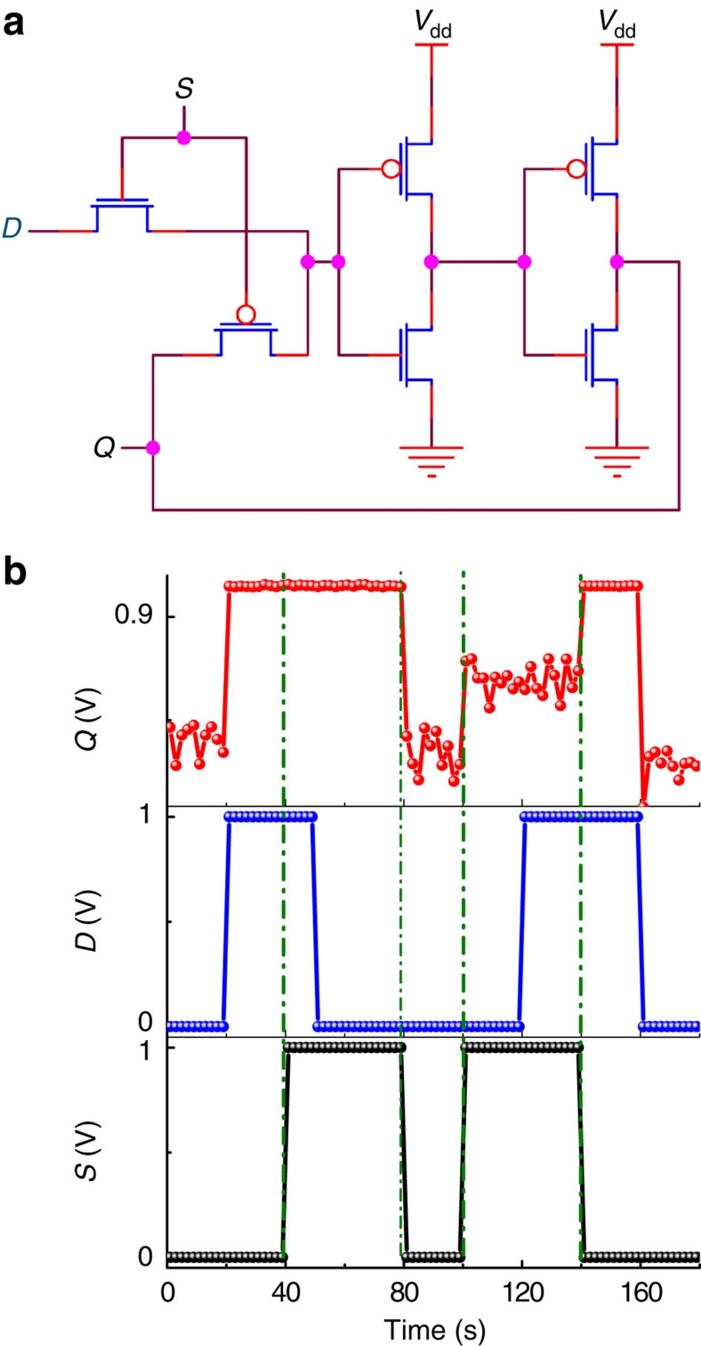
Field-effect transistors based on carbon nanotubes have been shown to be faster and less energy consuming than their silicon counterparts. However, ensuring these advantages are maintained for integrated circuits is a challenge. Here we demonstrate that a significant reduction in the use of field-effect transistors can be achieved by constructing carbon nanotube-based integrated circuits based on a pass-transistor logic configuration, rather than a complementary metal-oxide semiconductor configuration. Logic gates are constructed on individual carbon nanotubes via a doping-free approach and with a single power supply at voltages as low as 0.4 V. The pass-transistor logic configurarion provides a significant simplification of the carbon nanotube-based circuit design, a higher potential circuit speed and a significant reduction in power consumption. In particular, a full adder, which requires a total of 28 field-effect transistors to construct in the usual complementary metal-oxide semiconductor circuit, uses only three pairs of n- and p-field-effect transistors in the pass-transistor logic configuration.

摘要

基于碳纳米管的场效应晶体管被证明比其硅 counterparts 更快、能耗更低。然而,要确保这些优势在集成电路中得以保持,这是一个挑战。在这里,我们展示了通过构建基于传输晶体管逻辑配置的碳纳米管集成电路,而不是互补金属氧化物半导体配置,可以显著减少场效应晶体管的使用。逻辑门通过一种无掺杂的方法构建在单个碳纳米管上,并且在低至 0.4 V 的单个电源电压下工作。传输晶体管逻辑配置为碳纳米管基电路设计提供了显著的简化、更高的潜在电路速度和显著降低的功耗。特别是,全加器总共需要 28 个场效应晶体管才能在常用的互补金属氧化物半导体电路中构建,而在传输晶体管逻辑配置中仅使用三对 n 型和 p 型场效应晶体管。

https://cdn.ncbi.nlm.nih.gov/pmc/blobs/86fc/3293427/696d0562e1fe/ncomms1682-f8.jpg
https://cdn.ncbi.nlm.nih.gov/pmc/blobs/86fc/3293427/f326100926ca/ncomms1682-f1.jpg
https://cdn.ncbi.nlm.nih.gov/pmc/blobs/86fc/3293427/0796149e1d11/ncomms1682-f2.jpg
https://cdn.ncbi.nlm.nih.gov/pmc/blobs/86fc/3293427/e9233e241ef6/ncomms1682-f3.jpg
https://cdn.ncbi.nlm.nih.gov/pmc/blobs/86fc/3293427/dacc52114807/ncomms1682-f4.jpg
https://cdn.ncbi.nlm.nih.gov/pmc/blobs/86fc/3293427/86ad214c391a/ncomms1682-f5.jpg
https://cdn.ncbi.nlm.nih.gov/pmc/blobs/86fc/3293427/01b9573be051/ncomms1682-f6.jpg
https://cdn.ncbi.nlm.nih.gov/pmc/blobs/86fc/3293427/1ce8e6c06fd9/ncomms1682-f7.jpg
https://cdn.ncbi.nlm.nih.gov/pmc/blobs/86fc/3293427/696d0562e1fe/ncomms1682-f8.jpg

相似文献

1
CMOS-based carbon nanotube pass-transistor logic integrated circuits.基于 CMOS 的碳纳米管传输晶体管逻辑集成电路。
Nat Commun. 2012 Feb 14;3:677. doi: 10.1038/ncomms1682.
2
Subnanowatt carbon nanotube complementary logic enabled by threshold voltage control.亚纳瓦级碳纳米管互补逻辑由阈值电压控制实现。
Nano Lett. 2013 Oct 9;13(10):4810-4. doi: 10.1021/nl402478p. Epub 2013 Sep 12.
3
Scalable complementary logic gates with chemically doped semiconducting carbon nanotube transistors.具有化学掺杂半导体碳纳米管晶体管的可扩展互补逻辑门。
ACS Nano. 2011 Mar 22;5(3):2369-75. doi: 10.1021/nn200270e. Epub 2011 Mar 3.
4
Carbon nanotube field-effect transistors for use as pass transistors in integrated logic gates and full subtractor circuits.用于作为集成逻辑门和全减器电路中的传输晶体管的碳纳米管场效应晶体管。
ACS Nano. 2012 May 22;6(5):4013-9. doi: 10.1021/nn300320j. Epub 2012 Apr 13.
5
A 1 GHz integrated circuit with carbon nanotube interconnects and silicon transistors.一款带有碳纳米管互连和硅晶体管的1吉赫兹集成电路。
Nano Lett. 2008 Feb;8(2):706-9. doi: 10.1021/nl0730965. Epub 2008 Feb 13.
6
CMOS-analogous wafer-scale nanotube-on-insulator approach for submicrometer devices and integrated circuits using aligned nanotubes.用于亚微米器件和集成电路的基于绝缘层上纳米管的互补金属氧化物半导体类似物晶圆级方法,该方法使用排列的纳米管。
Nano Lett. 2009 Jan;9(1):189-97. doi: 10.1021/nl802756u.
7
Metal contact engineering and registration-free fabrication of complementary metal-oxide semiconductor integrated circuits using aligned carbon nanotubes.使用对齐的碳纳米管的金属接触工程和无注册互补金属氧化物半导体集成电路的制造。
ACS Nano. 2011 Feb 22;5(2):1147-53. doi: 10.1021/nn1027856. Epub 2011 Jan 27.
8
Strategy for carrier control in carbon nanotube transistors.碳纳米管晶体管中的载流子控制策略。
ChemSusChem. 2011 Jul 18;4(7):890-904. doi: 10.1002/cssc.201000412. Epub 2011 May 6.
9
High-Performance WSe2 Complementary Metal Oxide Semiconductor Technology and Integrated Circuits.高性能 WSe2 互补金属氧化物半导体技术与集成电路。
Nano Lett. 2015 Aug 12;15(8):4928-34. doi: 10.1021/acs.nanolett.5b00668. Epub 2015 Jul 28.
10
Metal--semiconductor transition in single-walled carbon nanotubes induced by low-energy electron irradiation.低能电子辐照诱导单壁碳纳米管中的金属-半导体转变
Nano Lett. 2005 Aug;5(8):1575-9. doi: 10.1021/nl0509935.

引用本文的文献

1
High-Performance Carbon Nanotube Electronic Devices: Progress and Challenges.高性能碳纳米管电子器件:进展与挑战。
Micromachines (Basel). 2025 May 1;16(5):554. doi: 10.3390/mi16050554.
2
Broadband plasmonic half-subtractor and digital demultiplexer in pure parallel connections.纯并行连接中的宽带等离子体半减法器和数字解复用器。
Nanophotonics. 2022 Jul 14;11(16):3623-3629. doi: 10.1515/nanoph-2022-0267. eCollection 2022 Sep.
3
Photoprogrammed Multifunctional Optoelectronic Synaptic Transistor Arrays Based on Photosensitive Polymer-Sorted Semiconducting Single-Walled Carbon Nanotubes for Image Recognition.

本文引用的文献

1
Carbon-Based Field-Effect Transistors for Nanoelectronics.用于纳米电子学的碳基场效应晶体管。
Adv Mater. 2009 Jul 13;21(25-26):2586-2600. doi: 10.1002/adma.200803582. Epub 2009 May 4.
2
Self-aligned U-gate carbon nanotube field-effect transistor with extremely small parasitic capacitance and drain-induced barrier lowering.自对准 U 型栅碳纳米管场效应晶体管,具有极小的寄生电容和漏极诱导势垒降低。
ACS Nano. 2011 Apr 26;5(4):2512-9. doi: 10.1021/nn102091h. Epub 2011 Mar 11.
3
Programmable nanowire circuits for nanoprocessors.可编程纳米线电路用于纳米处理器。
基于用于图像识别的光敏聚合物分类半导体单壁碳纳米管的光编程多功能光电突触晶体管阵列
Adv Sci (Weinh). 2024 Aug;11(29):e2401794. doi: 10.1002/advs.202401794. Epub 2024 Jun 3.
4
Controlled Preparation of Single-Walled Carbon Nanotubes as Materials for Electronics.作为电子材料的单壁碳纳米管的可控制备
ACS Cent Sci. 2022 Nov 23;8(11):1490-1505. doi: 10.1021/acscentsci.2c01038. Epub 2022 Nov 1.
5
Dielectrophoresis-Based Positioning of Carbon Nanotubes for Wafer-Scale Fabrication of Carbon Nanotube Devices.基于介电泳的碳纳米管定位用于碳纳米管器件的晶圆级制造。
Micromachines (Basel). 2020 Dec 25;12(1):12. doi: 10.3390/mi12010012.
6
Recent Progress in Inkjet-Printed Thin-Film Transistors.喷墨打印薄膜晶体管的最新进展
Adv Sci (Weinh). 2019 Jan 11;6(6):1801445. doi: 10.1002/advs.201801445. eCollection 2019 Mar 20.
7
Stable Logic Operation of Fiber-Based Single-Walled Carbon Nanotube Transistor Circuits Toward Thread-Like CMOS Circuitry.面向类线程互补金属氧化物半导体电路的基于光纤的单壁碳纳米管晶体管电路的稳定逻辑运算
Materials (Basel). 2018 Oct 1;11(10):1878. doi: 10.3390/ma11101878.
8
1D Piezoelectric Material Based Nanogenerators: Methods, Materials and Property Optimization.基于一维压电材料的纳米发电机:方法、材料与性能优化
Nanomaterials (Basel). 2018 Mar 23;8(4):188. doi: 10.3390/nano8040188.
9
Fabrication of a Low Density Carbon Fiber Foam and Its Characterization as a Strain Gauge.低密度碳纤维泡沫的制备及其作为应变片的特性研究
Materials (Basel). 2014 May 8;7(5):3699-3714. doi: 10.3390/ma7053699.
10
Solution-processed carbon nanotube thin-film complementary static random access memory.溶液处理碳纳米管薄膜互补静态随机存取存储器。
Nat Nanotechnol. 2015 Nov;10(11):944-8. doi: 10.1038/nnano.2015.197. Epub 2015 Sep 7.
Nature. 2011 Feb 10;470(7333):240-4. doi: 10.1038/nature09749.
4
Flexible high-performance carbon nanotube integrated circuits.柔性高性能碳纳米管集成电路。
Nat Nanotechnol. 2011 Mar;6(3):156-61. doi: 10.1038/nnano.2011.1. Epub 2011 Feb 6.
5
Length scaling of carbon nanotube transistors.碳纳米管晶体管的长度缩放。
Nat Nanotechnol. 2010 Dec;5(12):858-62. doi: 10.1038/nnano.2010.220. Epub 2010 Nov 21.
6
Anomalous Schottky barriers and contact band-to-band tunneling in carbon nanotube transistors.碳纳米管晶体管中的反常肖特基势垒和接触带带隧穿。
ACS Nano. 2010 Jun 22;4(6):3103-8. doi: 10.1021/nn100328a.
7
Growth and performance of yttrium oxide as an ideal high-kappa gate dielectric for carbon-based electronics.氧化钇作为碳基电子学中理想的高介电常数栅介质的生长和性能。
Nano Lett. 2010 Jun 9;10(6):2024-30. doi: 10.1021/nl100022u.
8
Y-contacted high-performance n-type single-walled carbon nanotube field-effect transistors: scaling and comparison with Sc-contacted devices.Y 接触高性能 n 型单壁碳纳米管场效应晶体管:与 Sc 接触器件的缩放比较。
Nano Lett. 2009 Dec;9(12):4209-14. doi: 10.1021/nl9024243.
9
Nanotube electronics for radiofrequency applications.用于射频应用的纳米管电子学。
Nat Nanotechnol. 2009 Dec;4(12):811-9. doi: 10.1038/nnano.2009.355. Epub 2009 Nov 29.
10
Almost perfectly symmetric SWCNT-based CMOS devices and scaling.基于近乎完美对称 SWCNT 的 CMOS 器件及缩放技术。
ACS Nano. 2009 Nov 24;3(11):3781-7. doi: 10.1021/nn901079p.